PCB Immersion Gold (ENIG) is a premium surface finish delivering excellent solderability, oxidation resistance, and flatness for high-reliability printed circuit boards. This guide explains definition, benefits, process, pros & cons, comparisons, and applications for engineers and global buyers.
What Is PCB Immersion Gold (ENIG) Surface Finish?
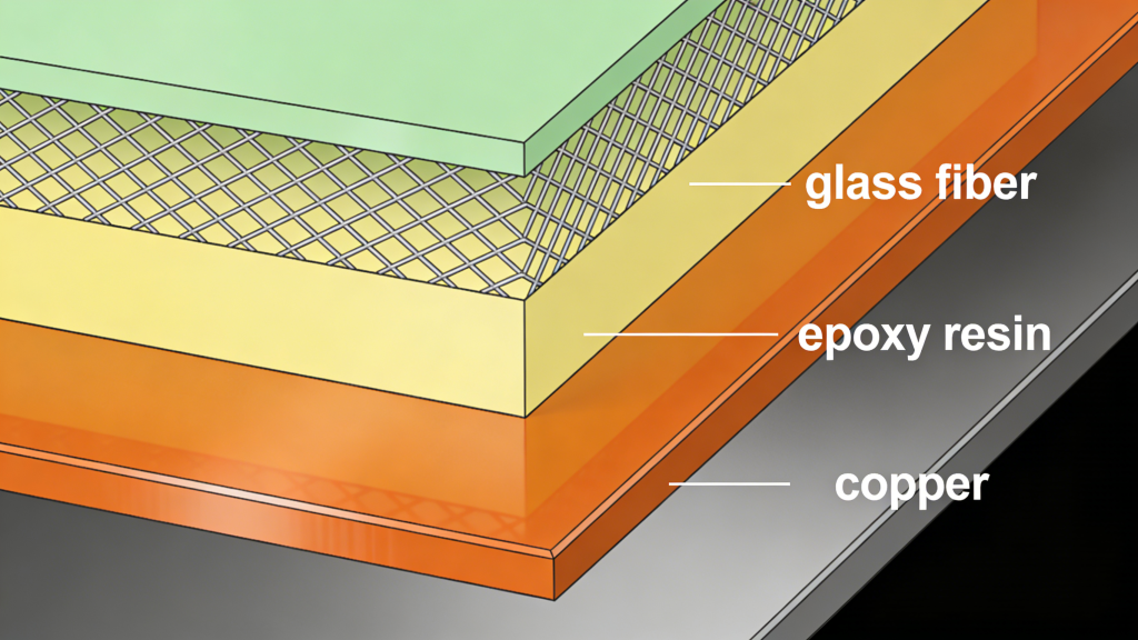
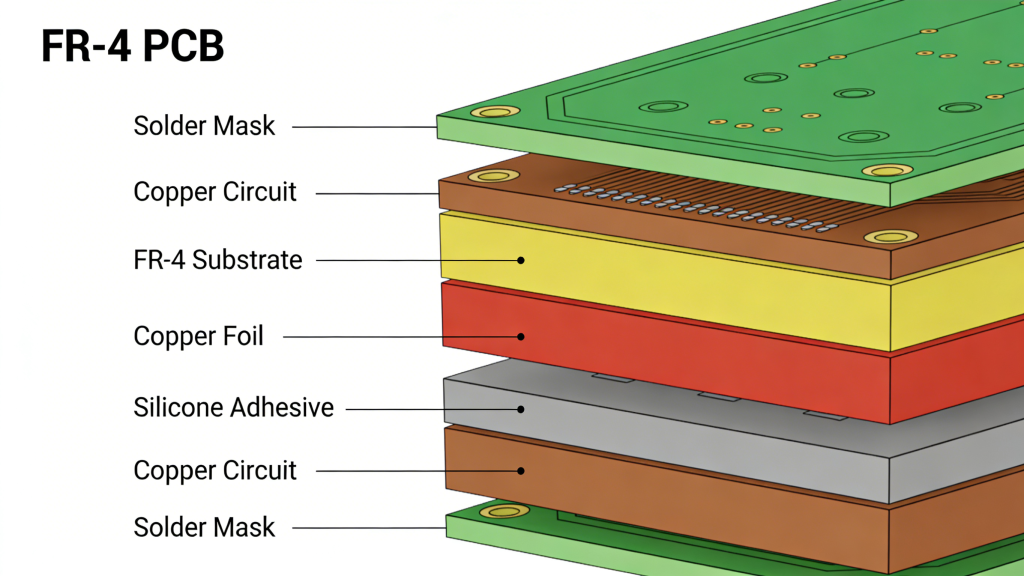
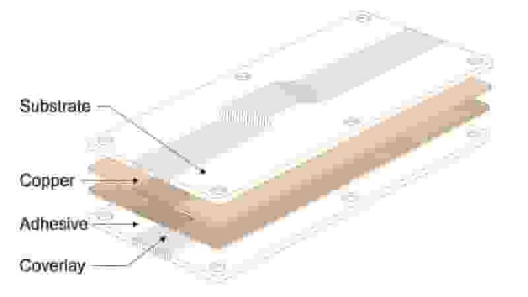
PCB Immersion Gold (ENIG) (Electroless Nickel Immersion Gold) is a two-layer chemical surface coating for printed circuit boards. It deposits a nickel-phosphorus base layer, then a thin immersion gold top layer to protect copper pads from oxidation and ensure stable soldering.
The gold layer is thin (0.05-0.15 μm), while nickel is 3-6 μm. This structure provides excellent flatness, ideal for BGA, QFN, flip-chip and high-density SMT assembly.
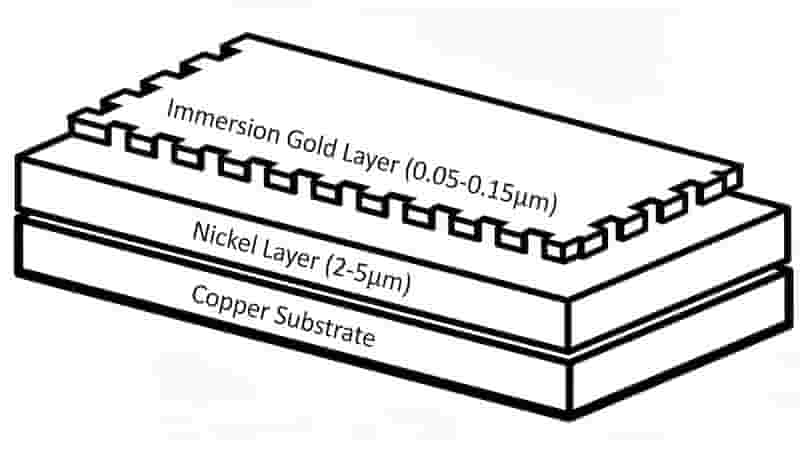
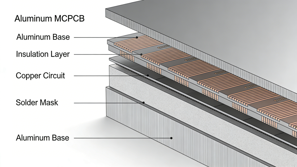
Layers of PCB Immersion Gold (ENIG) Surface Finish
Key Benefits of ENIG Surface Finish
- Excellent solderability for lead-free and SMT assembly
- Superior oxidation resistance and long shelf life
- Ultra-flat surface perfect for fine-pitch components and BGAs
- Stable electrical performance and contact reliability
- RoHS compliant, lead-free and environmentally safe
- Good thermal stability for reflow and wave soldering
- Works well for plated through-holes (PTH) and multilayer boards
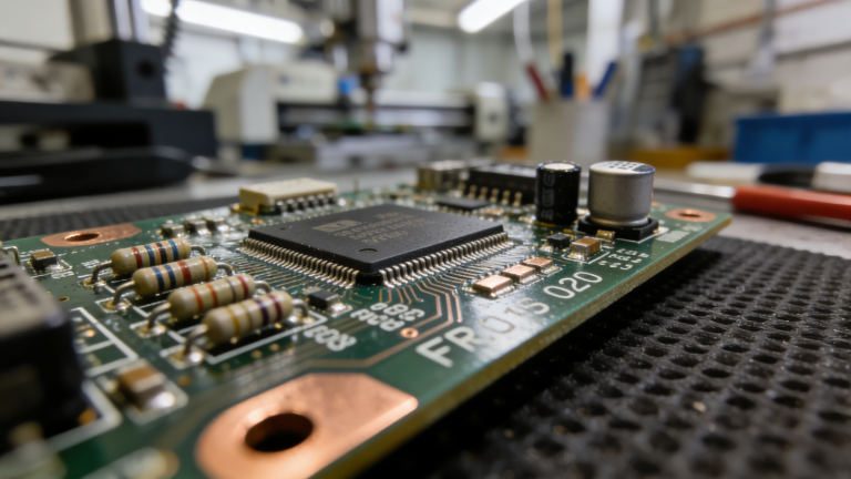
Typical Applications of ENIG PCBs
PCB Immersion Gold (ENIG) is widely used in high-reliability electronics:
- Consumer electronics: smartphones, tablets, laptops
- Automotive electronics: ECUs, sensors, lighting
- Medical devices: diagnostic and monitoring equipment
- Industrial control, IoT, 5G communication hardware
- High-precision SMT and fine-pitch PCB assemblies
Global Applications of PCB Immersion Gold (ENIG)
Disadvantages & Limitations of ENIG
- Higher cost than HASL, OSP, immersion silver
- Risk of black pad if process is poorly controlled
- Lower reworkability compared to some surface finishes
- Nickel may cause minor signal loss in ultra-high-frequency RF designs
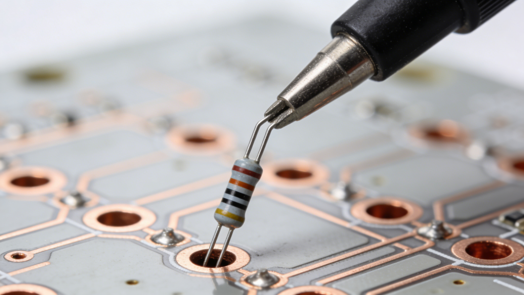
ENIG Manufacturing Process Step by Step
- Cleaning and surface preparation
- Micro-etching to activate copper pads
- Pre-dip and palladium activation
- Electroless nickel deposition (3-6 μm)
- Immersion gold plating (0.05-0.15 μm)
- Final rinsing, drying, and quality inspection
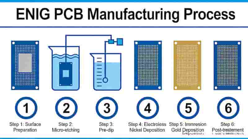
Standard PCB Immersion Gold (ENIG) Production Flow
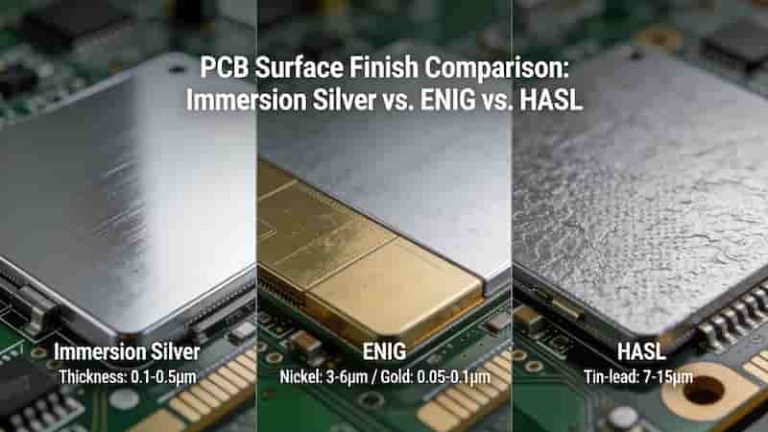
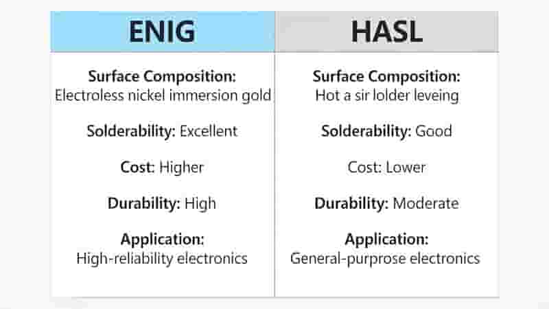
ENIG vs Other PCB Surface Finishes
| Surface Finish | Cost | Flatness | Oxidation Resistance | Best For |
|---|---|---|---|---|
| ENIG | Medium-High | Excellent | Excellent | BGA, fine-pitch, high-reliability |
| HASL | Low | Poor | Moderate | Cost-sensitive boards |
| OSP | Low | Good | Low | Short shelf-life assemblies |
| ENEPIG | Very High | Excellent | Excellent | High-frequency, bonding |
PCB Immersion Gold (ENIG) vs Other Finishes
Conclusion
PCB Immersion Gold (ENIG) is one of the most trusted surface finishes for high-performance, lead-free, and reliable printed circuit boards. It combines excellent flatness, strong solderability, long-term stability, and wide compatibility with modern SMT processes.
For critical applications in automotive, medical, industrial, and high-end consumer electronics, ENIG remains a top choice for engineers and international buyers.
Inquire About ENIG PCB Solutions
Need high-quality PCB Immersion Gold (ENIG) manufacturing, quotation, or custom PCB solutions? We provide reliable, cost-effective, and export-ready PCBs for global buyers.
Contact us today for a free quote and technical support!
Get Free Quote