This professional guide explains backdrilling of vias, how it removes via stubs to boost signal integrity, reduce EMI, and enable reliable high-frequency performance for advanced PCBs used in 5G, data centers, and high-speed electronics.
Introduction
With the exponential growth of high-speed applications such as 5G, autonomous vehicles, and IoT devices, PCBs are pushed to handle faster data rates and higher frequencies. This creates urgent demand for enhanced signal integrity, with backdrilling of vias emerging as a core solution.
Global search interest for backdrilled vias has risen by over 30% year over year, yet many designers and engineers lack clear insight into this critical process. We deliver professional, high-precision backdrilling of vias to support reliable, high-performance PCB manufacturing worldwide.
This guide covers definitions, comparisons, benefits, design rules, and manufacturing capabilities to help you make informed decisions for high-density, high-speed designs.
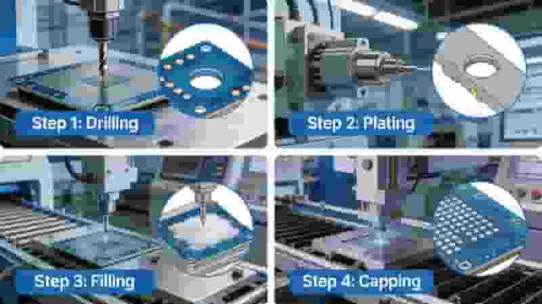
What Are Backdrilled Vias
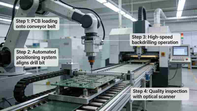
Backdrilled vias are precision-processed plated through-hole vias where the non-functional lower stub is removed after plating. Unlike standard vias that span the full board thickness, backdrilling of vias leaves only the required conductive path to target inner layers.
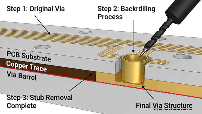
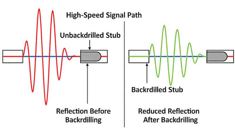
At high frequencies, via stubs cause parasitic impedance, signal reflection, and resonance. Backdrilling of vias eliminates these stubs to preserve clean transmission even at microwave and multi-GHz rates.
Benefits of Backdrilling Vias
Backdrilling of vias delivers measurable improvements for modern PCBs:
Improved Signal Integrity
Eliminates stub-induced reflections and distortion, ensuring clean signal transmission even at multi-gigabit data rates.
High-Speed Support
Enables stable transmission at 10Gbps+, 25Gbps+, and beyond, critical for 5G networks and data center interconnects.
Reduced EMI and Crosstalk
Lowers parasitic capacitance and noise coupling, significantly reducing electromagnetic interference between adjacent signal paths.
Higher Design Density
Supports HDI, high-layer-count, and BGA layouts by removing unnecessary via stubs that waste valuable board space.
Long-Term Reliability
Stabilizes impedance characteristics over temperature and time, essential for industrial and automotive applications.
Backdrilling Design Considerations
Effective backdrilling of vias requires careful planning to balance performance, cost, and manufacturability:
When to Use Backdrilling
- Recommended for signals above 3-5 GHz
- Ideal for BGAs, high-speed ICs, and RF paths
- Typically used on 6-12+ layer PCBs
Key Manufacturing Tolerances
- Depth tolerance: ±0.05 mm for industrial quality
- Minimum drill size: 0.15 mm for fine structures
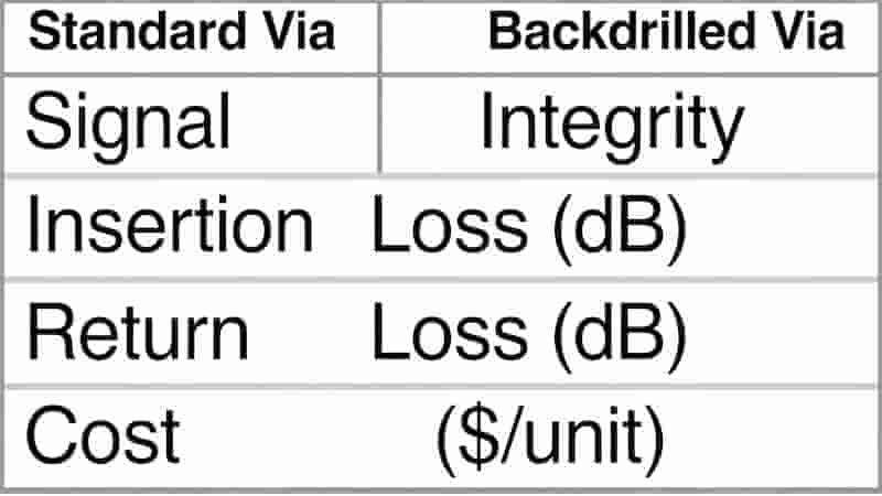
| Item | Standard Via | Backdrilled Via |
|---|---|---|
| Stub Length | Full board thickness | ≤50 μm / 2-8 mil |
| High-Speed Performance | Limited | Excellent for multi-GHz |
| EMI Radiation | High | Significantly reduced |
| Best For | Low-speed PCBs | High-speed / RF PCBs |
Our Backdrilling Capabilities
We provide industry-leading backdrilling of vias for global PCB buyers, engineers, and procurement teams:
- Via Types: Plated through-hole, blind, and buried vias
- Precision: Depth accuracy ±0.05 mm; min hole 0.15 mm
- Layer Support: Up to 30+ layers for high-end systems
- Engineering: DRC, stackup optimization, and SI review
- Quality: Impedance testing, cross-section, and network analysis
Conclusion
Backdrilling of vias is no longer optional for high-performance PCBs. It is essential for 5G, data centers, automotive radar, test equipment, and other multi-GHz applications where signal integrity directly determines product success.
Our advanced fabrication and engineering team ensures your PCBs achieve optimal speed, density, and reliability with controlled backdrilling of vias.
Get Expert Backdrilling Support for Your PCB Project
Send us your Gerber files, layer stackup, and speed requirements for a free DFM check and precise quote.
Contact us today for custom backdrilling solutions, fast prototyping, and volume production.