PCB vias are essential vertical interconnects in multilayer PCBs that link copper layers for signal, power, and ground paths. This professional guide explains through vias, blind vias, and buried vias with engineering specs, manufacturing processes, and real-world use cases to help engineers and buyers select reliable via solutions.
What Are PCB Vias?
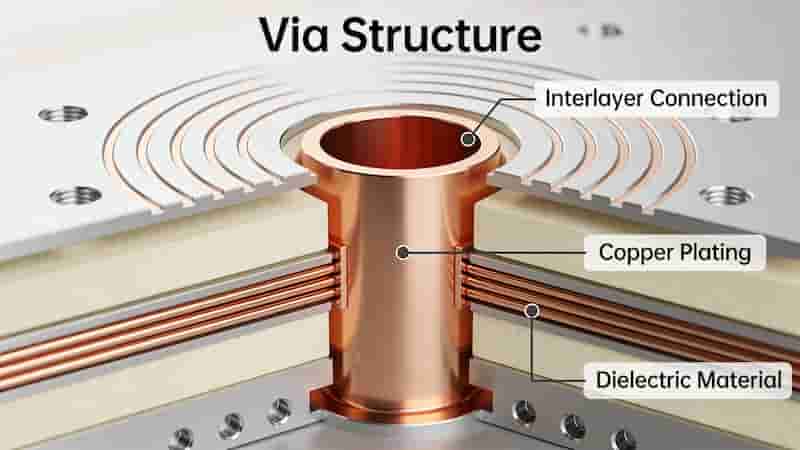
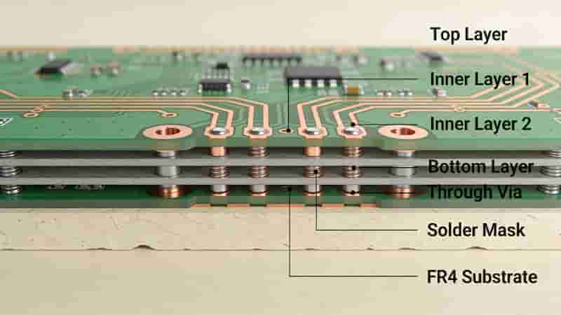
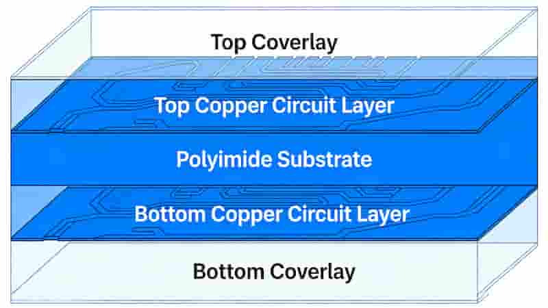
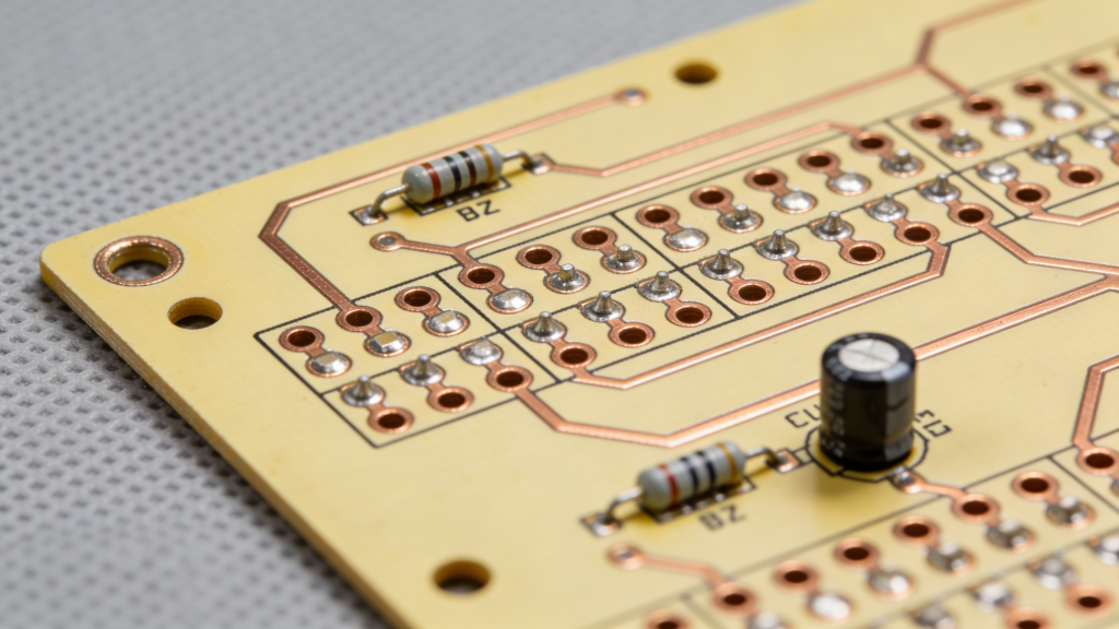
A PCB via is a plated conductive hole that creates electrical connections between different copper layers in multilayer printed circuit boards. Since copper layers are separated by insulating materials, vias are critical components for signal transmission, power delivery, and grounding in modern electronics.
Without stable PCB vias, complex circuits cannot operate efficiently. They are widely used in automotive systems, medical devices, 5G infrastructure, industrial controls, and high-performance consumer electronics.
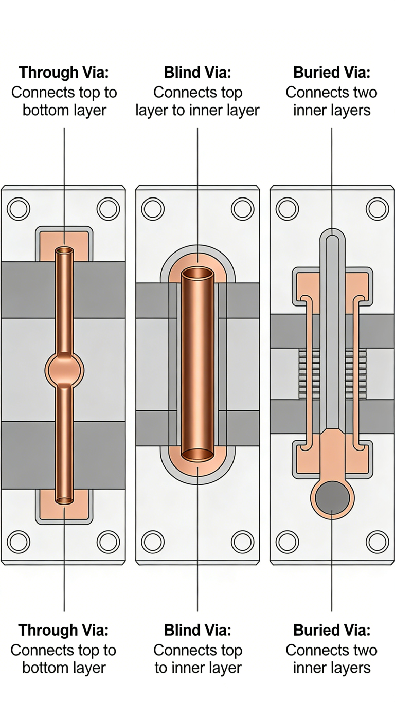
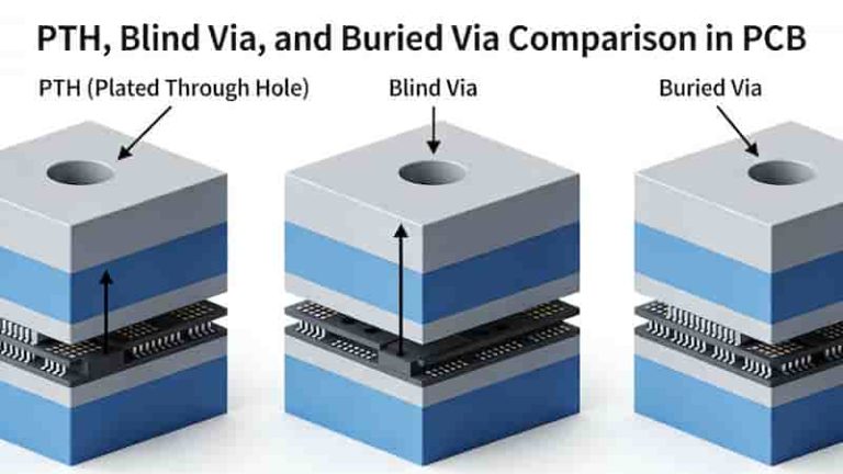
Through Vias (Plated Through Holes)
Through vias are the most common and cost-effective via type. They penetrate the entire PCB thickness and connect all outer and inner layers with a fully plated copper wall.
- Minimum drill diameter: 0.15 mm (6 mil)
- Manufacturing: Mechanical drilling + electroplating
- Best use: Standard PCBs, through-hole components, power circuits
- Advantages: Low cost, high reliability, easy mass production
- Limitations: Occupies more surface area, not ideal for HDI designs
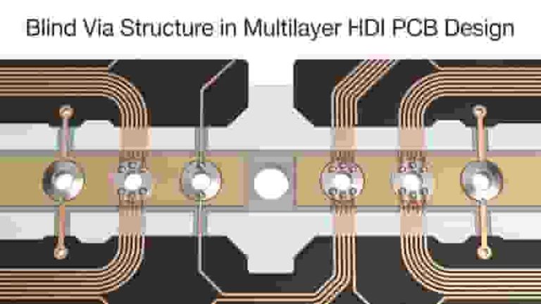
Blind Vias
Blind vias connect an outer layer to one or more inner layers but do not pass through the entire PCB. They are widely used in HDI and high-speed PCB designs.
- Minimum drill diameter: 0.1 mm (4 mil)
- Manufacturing: Laser drilling with precise depth control
- Best use: High-density PCBs, smartphones, wearables, high-speed circuits
- Advantages: Saves routing space, improves signal integrity
- Limitations: Higher cost, requires advanced fabrication equipment
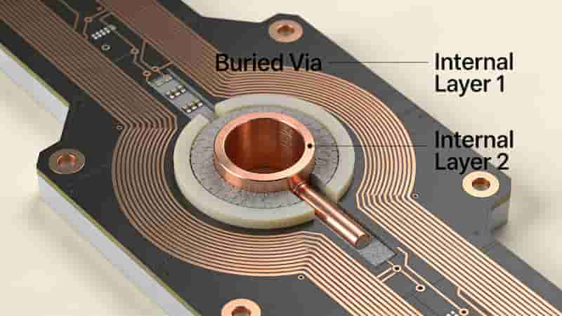
Buried Vias
Buried vias connect only internal copper layers and remain completely hidden inside the PCB with no exposure on outer surfaces.
- Minimum drill diameter: 0.1 mm (4 mil)
- Manufacturing: Drilled before lamination, laser precision
- Best use: High-layer-count PCBs, servers, aerospace, medical electronics
- Advantages: Maximizes routing space, reduces parasitic capacitance
- Limitations: Complex process, highest manufacturing cost
PCB Via Type Comparison
| Parameter | Through Via | Blind Via | Buried Via |
|---|---|---|---|
| Layer Connection | All layers | Outer to inner | Inner only |
| Minimum Size | 0.15 mm | 0.1 mm | 0.1 mm |
| Manufacturing Cost | Lowest | Medium | Highest |
| Best Application | Standard PCBs | HDI PCBs | High-layer PCBs |
Via Design & Manufacturing Guidelines
Professional PCB fabrication requires strict via design rules to ensure long-term reliability and electrical performance:
- Follow IPC standards for via size, aspect ratio, and copper plating thickness
- Use laser drilling for blind and buried vias in HDI PCBs
- Control depth-to-diameter ratio for uniform plating quality
- Optimize via placement to reduce signal crosstalk and interference
- Select via type based on layer count, signal speed, and project budget
Conclusion
Understanding through vias, blind vias, and buried vias is essential for designing reliable, high-performance PCBs. Choosing the right via type improves functionality, optimizes cost, and meets industry standards for modern electronic devices.
Whether you need standard PCBs with through vias or advanced HDI PCBs with blind and buried vias, professional manufacturing ensures stable quality and performance for global industrial applications.
Get Expert PCB Manufacturing Support
Contact us for PCB design review, via optimization, custom fabrication, and detailed quotes for your industrial and commercial projects.
Request a Free Quote
Double-Sided Flex PCB Manufacturing Services | 2-Layer Flexible PCB Solutions
How to Choose a Reliable PCB Prototype Manufacturer for Electronics Projects
Metal Core PCB (MCPCB) Manufacturing Service in China
Single Layer PCB Manufacturing | Affordable Single Sided PCBs
Nano-Coated PCB Stencil Manufacturing for Precision & Durability