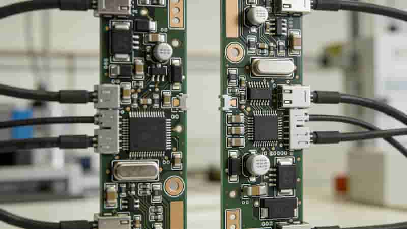
Plated Through Holes (PTH) are essential conductive structures in PCBs that ensure stable interlayer connectivity, reliable component mounting, and long‑term performance for industrial and high‑reliability electronics.
What Are Plated Through Holes (PTH)
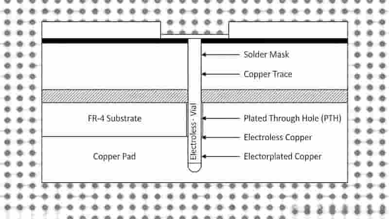
A Plated Through Hole (PTH) is a drilled hole in a printed circuit board whose inner walls are coated with a conductive metal layer—typically copper—to create a permanent electrical connection between the top, inner, and bottom layers of the PCB.
Unlike non‑plated holes, PTH forms a continuous conductive barrel that supports through‑hole component mounting and stable layer interconnection in multilayer PCBs.
Key Benefits of PTH in PCBs
1. Stable Interlayer Connectivity: PTH provides consistent electrical paths across all layers, ideal for multilayer PCB designs.
2. Reliable Component Mounting: Supports through‑hole components used in industrial, automotive, and high‑vibration environments.
3. Superior Mechanical Strength: Plated walls strengthen holes against thermal stress and physical shock.
4. Design Flexibility: Enables routing and component placement on both sides of the board.
5. High Signal Integrity: Low resistance and stable connection preserve signal quality.
Critical PTH Design Considerations
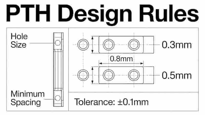
Hole Size
Must match component lead diameter. Common range: 0.3 mm – 0.8 mm. Too small blocks insertion; too large reduces reliability.
Hole Spacing
Minimum spacing ≥ 2 × finished hole diameter after plating to avoid short circuits.
Aspect Ratio (Depth / Diameter)
High aspect ratios increase plating difficulty and cost. Keep ratio within manufacturing capabilities.
Layer Count & Depth
Full‑depth PTH connects all layers. Partial depth may reduce cost for specific interlayer connections.
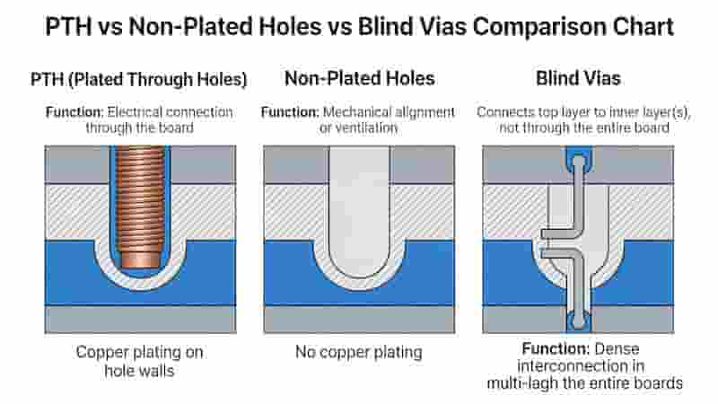
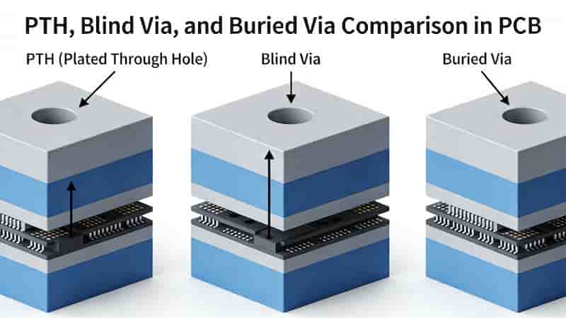
PTH vs Non‑Plated Holes vs Blind & Buried Vias
| Feature | Plated Through Holes (PTH) | Non‑Plated Holes | Blind / Buried Vias |
|---|---|---|---|
| Conductivity | Continuous conductive barrel | Non‑conductive | Plated partial layers |
| Connection | All layers | Mechanical only | Partial inner/outer layers |
| Reliability | Excellent | Low | High |
| Cost | Medium | Low | High |
| Best For | Multilayer PCB, through‑hole components | Mounting, no electrical need | High‑density PCB, compact designs |
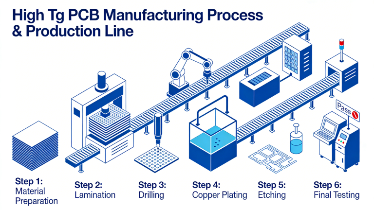
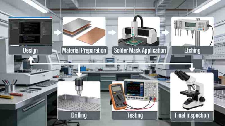
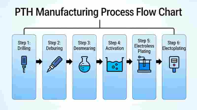
Standard PTH Manufacturing Process
1. Drilling: Precision drilling of through holes in the PCB core.
2. Desmear: Removal of resin smear to ensure plating adhesion.
3. Electroless copper deposition: Base conductive layer on hole walls.
4. Electroplating: Thickening copper layer to meet conductivity requirements.
5. Panel plating, etching, and solder mask application.
Conclusion
Plated Through Holes (PTH) are foundational to reliable printed circuit board design, especially for multilayer boards, through‑hole components, and industrial‑grade applications. Proper PTH design—including hole size, spacing, and aspect ratio—directly impacts PCB performance, reliability, and cost.
For mission‑critical, high‑temperature, or high‑vibration environments, PTH remains the most trusted interconnection solution.
Inquiry & Custom PCB Service
We specialize in professional PCB manufacturing with high‑quality Plated Through Holes (PTH) for global industrial buyers, engineers, and procurement teams.
If you need PTH PCB fabrication, custom design support, prototype validation, or bulk production, please contact us for a free quotation and technical proposal.
Request PTH PCB Quote Now
Blind Vias & Buried Vias in PCBs – The Complete Technical Guide
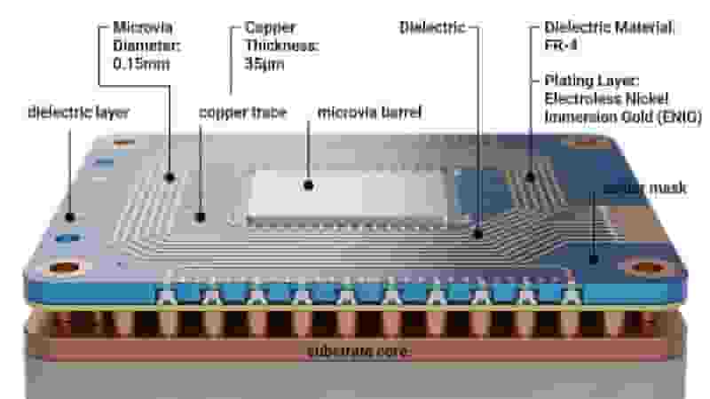
The Essentials of Microvias – Enabling Miniaturization in PCBs
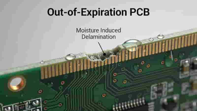
Out-of-Expiration PCB: Risks, Failures and Safe Handling Guidelines
Turnkey PCB Assembly Services | Full & Partial Solutions
Through-hole PCB Assembly Service | IPC Certified THT PCBA Solutions
Double Sided PCB Assembly: Full Process, Advantages & Manufacturing Guide
FAQs About Plated Through Hole(PTH) PCB Design & Production
Q: What is PTH plated through hole?
A: PTH is drilled through-hole with copper plated on inner barrel, forming continuous conductive path linking top, inner and bottom PCB layers for electric connection and component soldering.
Q: Main advantages of PTH structure on PCB?
A: Stable interlayer conduction, solid mechanical fixation for through-hole parts, good shock & thermal resistance and flexible double-side layout routing.
Q: Common finished hole size range for standard PTH?
A: Normal finished hole diameter ranges from 0.3mm~0.8mm, matched with corresponding component lead dimension.
Q: Difference among PTH, non-plated hole and blind/buried via?
A: PTH conducts across all layers; non-plated hole only for mechanical fixing without conduction; blind/buried via connects partial layers with high cost for high-density layout.
Q: What is PTH aspect ratio and its influence?
A: Aspect ratio = hole depth / hole diameter; excessive ratio raises plating difficulty, increases cost and easily causes incomplete copper plating inside barrel.
Q: Key production steps for PTH fabrication?
A: Precision drilling → desmear cleaning → electroless copper base plating → electroplating copper thickening → subsequent etching & solder mask processing.
Q: Which applications prefer PTH design?
A: Multilayer PCBs, industrial control, automotive and high-vibration equipment requiring reliable through-hole component mounting.
Q: How to set minimum spacing between adjacent PTH?
A: Keep hole spacing ≥ twice of finished hole diameter after plating to avoid copper short circuit between holes.