Single-sided flexible PCBs look simple, but poor design on bending radius, trace layout or stiffener placement can quickly lead to cracks and failures. This engineering guide provides practical rules for minimum bend radius, trace routing in flex zones, and stiffener usage to keep single-sided flexible PCB reliable in static and dynamic applications.
Introduction to Single-Sided Flexible PCB Design
Single-sided flexible PCBs look simple compared to multilayer or rigid-flex designs, but their success still depends heavily on good mechanical and layout design decisions.. Even with only one copper layer, bend radius, trace routing and stiffener placement determine whether a single-sided flexible PCB performs reliably over its lifetime or fails early.
In design terms, a single-sided flexible PCB is built on a thin polyimide base film with copper on one side, patterned into traces and pads. Its flexibility allows bending, folding and twisting to fit 3D spaces, replace wire harnesses, and fit into tight enclosures.
Bending radius, trace routing and stiffeners are the three most critical factors for mechanical reliability. A too-small bend radius strains copper and polyimide until cracking occurs. Poor routing concentrates stress, while misplaced stiffeners create rigid edges that accelerate fatigue.
Common failures from weak flex design include copper trace cracking, pad lifting, delamination, and intermittent open circuits. Most issues come from underestimated bend radius, bad trace direction, missing strain relief, or late collaboration with manufacturers.
Material Selection and Stackup
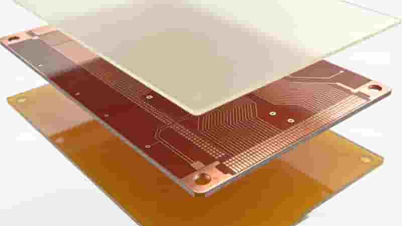
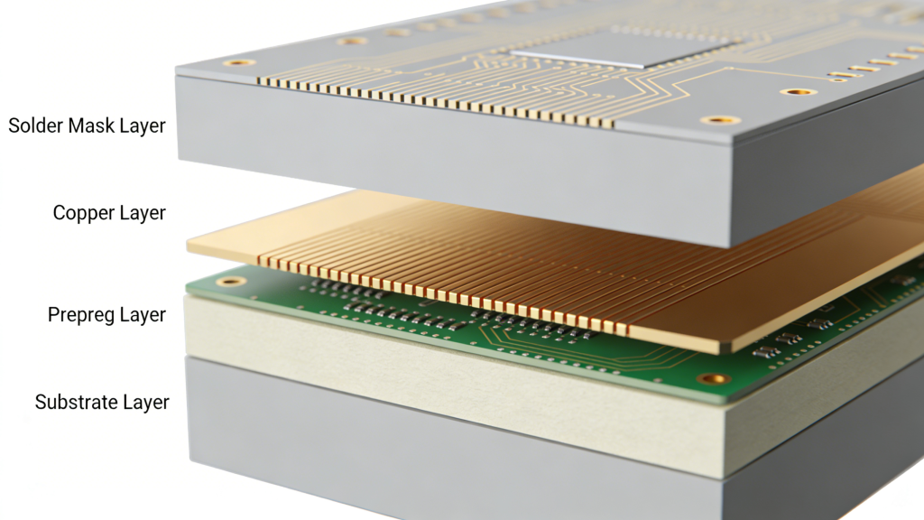
Material and stackup directly influence bendability, reliability, and cost for a single-sided flexible PCB. The combination of polyimide, copper, adhesive and coverlay defines long-term performance under bending and thermal cycling.
Most designs use polyimide (PI) base film with rolled annealed (RA) or electro-deposited (ED) copper. RA copper offers better ductility for dynamic flexing, while ED copper lowers cost for static applications. Thinner PI and copper reduce bend radius but reduce tear resistance.
Flex circuits use coverlay instead of solder mask. Coverlay is a PI film with adhesive laminated over copper for better flexibility. Adhesive or adhesiveless structures are chosen based on temperature, flexibility, and budget.
A standard stackup is PI core + copper + circuit + coverlay. Stiffeners can be added locally for component support without losing overall flexibility.
Bending Radius Design Rules
The bending radius is the most important mechanical parameter for single-sided flexible PCB reliability. The basic formula is R = t × N, where R = bend radius, t = total flex thickness, N = safety factor.
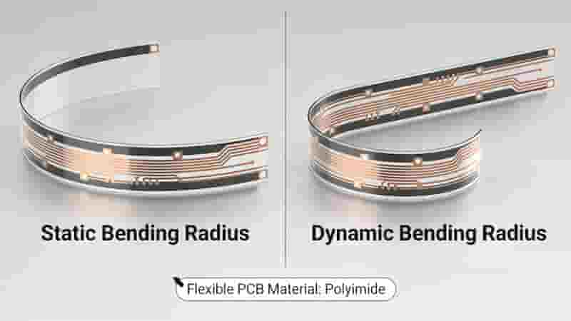
For static bending (one-time assembly): use 6–10× total thickness. For dynamic bending (repeated cycles): use 50–100× thickness to avoid fatigue failure.
Reduce stress by keeping bend regions thin, avoiding sudden thickness changes, using gradual curves, and maintaining uniform copper distribution. Always validate with your manufacturer.
Trace Routing Guidelines in Flex Areas
Proper routing preserves mechanical and electrical performance for a single-sided flexible PCB. The goal is to reduce stress while meeting signal requirements.
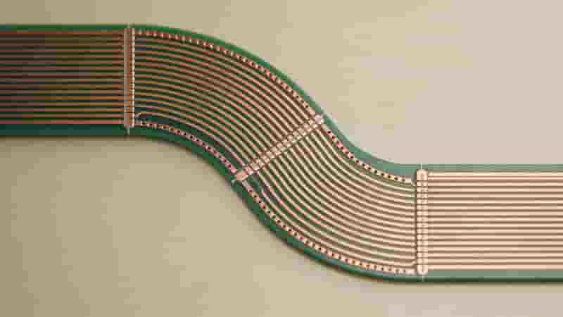
Route traces perpendicular to bend lines to distribute stress evenly. Avoid parallel routing, which causes concentrated tension and cracking.
Use wider traces in dynamic zones for longer fatigue life. Maintain consistent spacing and uniform copper distribution. Replace sharp 90° corners with rounded arcs or chamfers. Use teardrops at pad-trace joints to lower stress concentration.
Vias, Pad and Component Placement
Rigid features like vias and components must be placed carefully to protect single-sided flexible PCB integrity.
Keep vias, plated holes, and mounting holes away from bend lines. Use rounded pads and teardrops to prevent lifting. Extend coverlay to anchor pads securely.
Place all components and connectors in non-bending areas supported by stiffeners. Heavy components and connectors create excessive stress if placed in flex zones.
Using Stiffeners in Single-Sided Flex PCBs
Stiffeners provide rigid mounting areas while keeping the rest of the single-sided flexible PCB flexible. They protect solder joints and improve assembly stability.
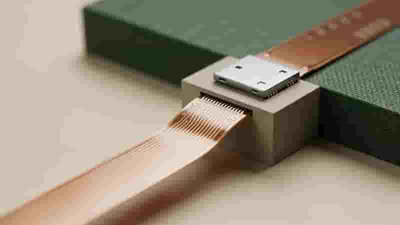
Use stiffeners under connectors, components, and mounting areas. Common materials: FR4 (low cost), PI (thin flexible), aluminum (thermal), stainless steel (high strength).
Stiffeners must fully support component footprints but not end exactly at bend lines. Leave a small transition zone to avoid sharp hinge stress.
Static vs Dynamic Flex Design Comparison
| Parameter | Static Bending | Dynamic Bending |
|---|---|---|
| Bending Radius | 6–10× thickness | 50–100× thickness |
| Copper Type | ED or RA | RA Copper Preferred |
| Trace Width | ≥4 mil | ≥6–8 mil |
| Stiffener Need | Standard | Reinforced Required |
DFM and Collaboration with Manufacturer
Early DFM review prevents failures and redesigns for single-sided flexible PCB projects. We verify bend radius, stackup, trace rules, coverlay, and stiffener placement to match real production capability.
Provide stackup specs, bend locations, static/dynamic notes, mechanical drawings, BOM, and assembly requirements. Early alignment reduces iterations and improves reliability.
Practical Design Checklist
Bend Radius & Thickness
- Confirm total thickness for each bend zone
- Use 6–10× for static, 50–100× for dynamic flex
- Avoid thickness steps at bend lines
Trace Routing & Vias
- Route perpendicular to bend lines
- Use rounded corners and teardrops
- Keep vias away from high-strain bend areas
Pads, Components & Stiffeners
- Use rounded pads and anchored coverlay
- Place components only in stiffened non-bend areas
- Stiffeners support full footprints without ending at bends
Conclusion & Next Steps
A reliable single-sided flexible PCB requires correct bending radius, proper trace routing, and strategic stiffener use. Following IPC and industry best practices drastically reduces failures in static and dynamic applications.
We specialize in custom single-sided flexible PCB design, prototyping, and mass production for global industrial buyers, engineers, and procurement teams. We provide free DFM checks and professional design support.
Get Your Custom Single-Sided Flex PCB Solution
Send your Gerber, BOM, and bending requirements for a free DFM review and formal quote.
Request Free Quote Now

PCB Classification Guide: Types, Applications & Selection for Industrial Buyers
What is a PCB BOM and How to Create One
Standard PCB Thickness: Complete Guide for Engineers & Buyers
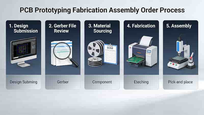
How to Order PCB Prototyping, Fabrication & Assembly Services in China
What Is the Difference Between PCB and PCBA? A Complete Guide for Industrial Buyers