HDI PCB structure cross section with microvias and fine traces

HDI PCB Layout and Basic HDI Design Guidelines 

This professional guide covers HDI PCB layout practices, stack-up, microvias, routing rules, DFM, impedance control and IPC standards to help engineers and procurement teams build reliable, mass-producible HDI PCB for high-speed, miniaturized electronics.

What Is HDI PCB Layout

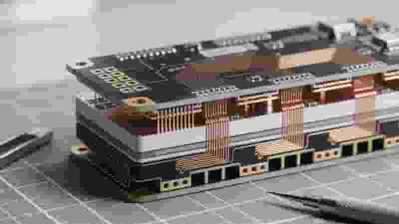
HDI PCB (High-Density Interconnect) layout refers to design methods used when trace widths drop below 8 mils (0.2 mm). It allows higher component density, smaller board size, and better electrical performance for modern electronics.

HDI PCB structure cross section with microvias and fine traces

Key Features of HDI PCB

A typical HDI PCB includes these critical characteristics to support high-density designs:

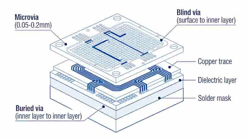
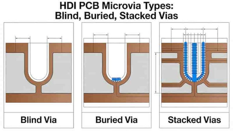
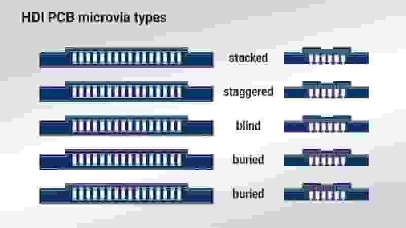
  • Microvias (laser-drilled blind & buried vias)
  • Fine traces: 3–5 mils for high wiring density
  • Thin dielectric layers for impedance control
  • High layer counts up to 20+ layers for complex systems
  • Low signal loss design for high-speed circuits

Trace & Via Design for HDI PCB

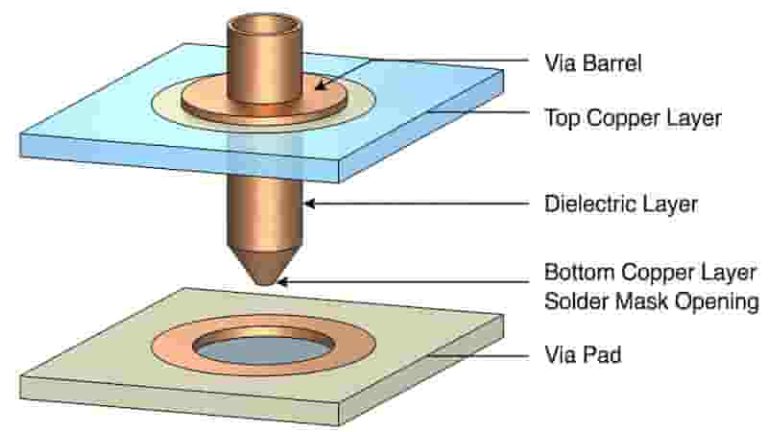
Vias are the most critical part of HDI PCB layout. Through-hole vias are rarely used; microvias with aspect ratio ≤ 1:1 are preferred for reliability.

  • Microvia diameter: 2–4 mils (50–100 μm)
  • Stacked & staggered vias for layer transitions
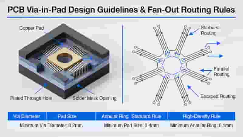
  • VIPPO (Via-in-Pad Plated Over) for fine-pitch BGAs
  • Follow IPC-2221A for aspect ratio limits
HDI PCB microvia types stacked staggered blind buried

Basic HDI Design Guidelines

These universal rules apply to all HDI PCB layout projects to ensure manufacturability and performance:

  • Confirm your manufacturer’s capabilities before design
  • Maintain consistent trace spacing and impedance
  • Avoid unnecessary ELIC or complex via structures
  • Use minimal layer count to reduce cost
  • Prioritize signal integrity for high-speed designs
HDI PCB layout design guidelines for engineers

BGA Fanout & Routing in HDI PCB Layout

Fine-pitch BGAs require specialized fanout strategies in HDI PCB design:

  • 0.8 mm pitch: Dogbone fanout with microvias
  • 0.5–0.75 mm pitch: VIPPO (via-in-pad)
  • Route between pads only if traces ≤ 4 mils are supported
HDI PCB BGA fanout dogbone vippo routing

DFM Rules for HDI PCB

DFM (Design for Manufacturing) ensures your HDI PCB layout can be produced with high yield and stable quality.

  • Match trace/space to factory capabilities
  • Use valid solder mask clearances
  • Include test points for electrical testing
  • Follow IPC-6012 for quality classification

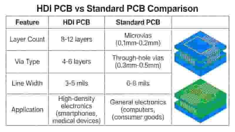
HDI PCB vs Standard PCB

ItemHDI PCBStandard PCB
Trace Width3–5 mils≥6 mils
Via TypeMicrovia, Blind, BuriedThrough-hole
DensityUltra HighStandard
Application5G, AI, Automotive, MobileIndustrial, Power, Control

Conclusion

Following professional HDI PCB layout and design guidelines is essential for creating reliable, cost-effective, and mass-producible HDI boards. Correct via design, impedance control, and DFM compliance directly improve yield and performance.

HDI PCB finished assembly for industrial electronics

Get Your HDI PCB Solution

We provide professional HDI PCB manufacturing, assembly and design support for global buyers. Request a free quote now.

Request HDI Quote

PCB Prototype Global Export and Service

PCB Prototype Manufacturing in China: Benefits, Challenges & Reliable Solutions

Posted on
0 Comments
PCB prototype manufacturing in China delivers exceptional cost efficiency, fast lead times, advanced engineering capabilities, and scalable production for global electronics buyers. This guide breaks down key advantages, common risks, and how to secure consistent quality for your prototype projects. Introduction to PCB Prototype Manufacturing in China Printed Circuit Boards (PCBs) are the core of…
SMT Reflow Soldering Oven for PCB Manufacturing

What is SMT Assembly? A Complete Guide for Industrial PCB Buyers & Engineers

Posted on
0 Comments
SMT assembly (Surface Mount Technology) is the core process in modern electronics manufacturing, used to mount components directly onto PCB surfaces for miniaturization, high density, automation, and reliable mass production. This guide explains processes, components, equipment, applications, and best practices for global industrial buyers. What Is SMT Assembly? SMT assembly is a high‑precision manufacturing method…
PCB reliability definition and functional carrier structure for industrial PCBA

Why PCB Reliability Is Critical for Industrial & Global Electronics Applications

Posted on
0 Comments
PCB reliability ensures stable performance, long service life, and safety for PCBA and end products. High‑reliability PCBs reduce failures, lower costs, and strengthen global market competitiveness. What Is PCB Reliability? Reliability means a product can consistently perform its intended function under defined conditions and within a specified lifetime. For end products, higher reliability directly means…
Flex PCB for 6G Communication and Robotics Applications

Top Applications of Flexible Printed Circuit Boards in 2025

Posted on
0 Comments
Flexible printed circuit boards (Flex PCBs) are reshaping the 2025 electronics industry with superior flexibility, lightweight design, and high reliability. Widely used in wearables, medical devices, automotive electronics, IoT, aerospace, and 6G systems, flex PCBs enable miniaturization, durability, and high‑speed signal transmission. We provide professional flex PCB solutions for global industrial buyers, engineers, and procurement…
Circuit schematic design for PCB layout

Ultimate Guide to Converting Circuit Diagrams to PCB Layouts for Engineers & Buyers

Posted on
0 Comments
Discover the essential steps to convert circuit diagrams into optimized PCB layouts. We share professional insights on tools, common pitfalls, and advanced techniques to ensure your designs are manufacturable and high-performing. Ideal for engineers seeking reliable PCB prototype and assembly services. In the fast-paced world of electronics, turning a conceptual circuit diagram into a functional…
SMT PCB AOI and X-ray Inspection Equipment

Surface Mount Technology (SMT) PCB Assembly Service

Posted on
0 Comments
Surface Mount Technology (SMT) PCB Assembly Service mounts electrical components directly onto the surface of printed circuit boards without through-hole leads. As a leading assembly solution for modern electronics, it delivers compact size, high reliability, and cost efficiency for industrial, medical, automotive, and consumer products worldwide. We provide one-stop service covering PCB production, component sourcing,…

Similar Posts