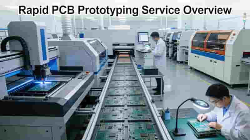
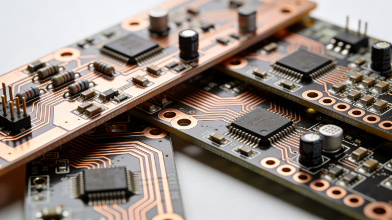
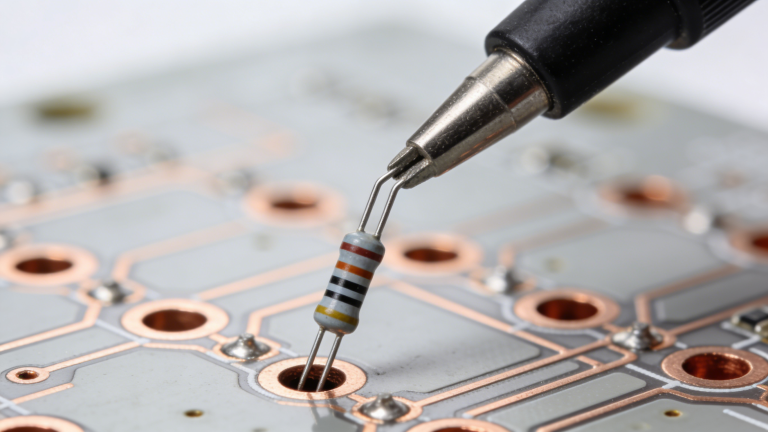
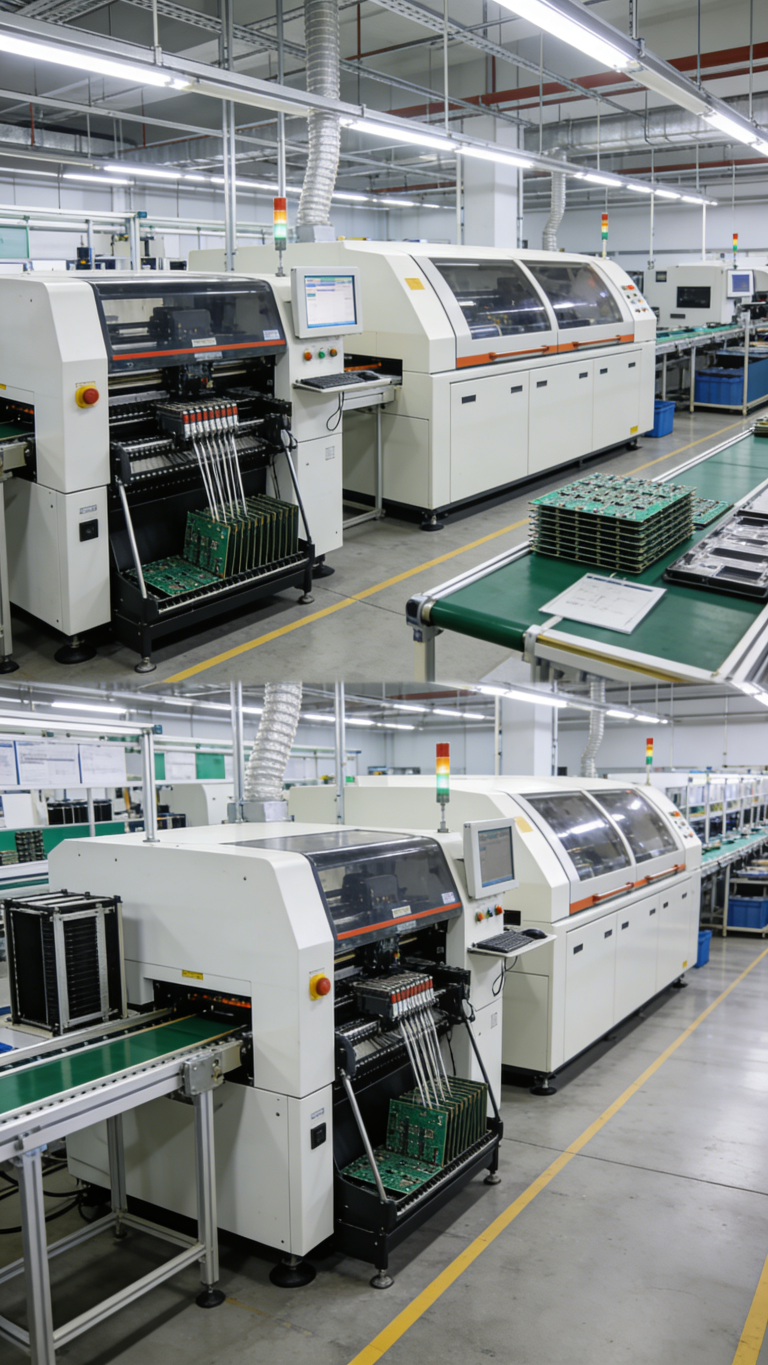
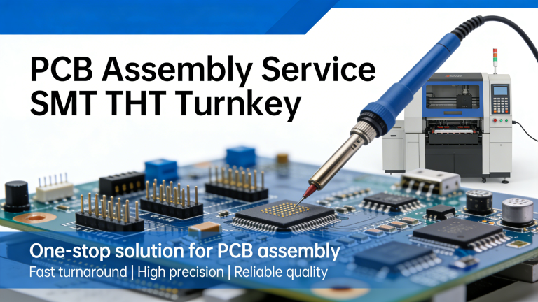
Get a clear quote within 24 hours and receive high-quality PCB prototypes in as fast as 3-5 days, with one-to-one engineering support from inquiry to delivery.
Get a Free Quote Now
24h quotation · 3-5 day PCB prototyping · One-stop PCB & PCBA
Why Engineers and Buyers Choose Us
From fast PCB prototypes to full production and turnkey assembly, we help you place orders with clearer communication, dependable quality, and competitive China-based manufacturing support.
Competitive Pricing
Our China-based production reduces overall PCB and PCBA costs while maintaining responsive service and reliable quality for prototypes and volume orders.
Fast Turnaround
Quick quotation, flexible quantities, and fast lead times: standard prototypes in 3-5 days, with quick-turn options for urgent projects.
Stable Quality Control
Over 20 years of experience, IPC Class 2/3 capability, AOI and X-ray inspection to meet standards for demanding applications.
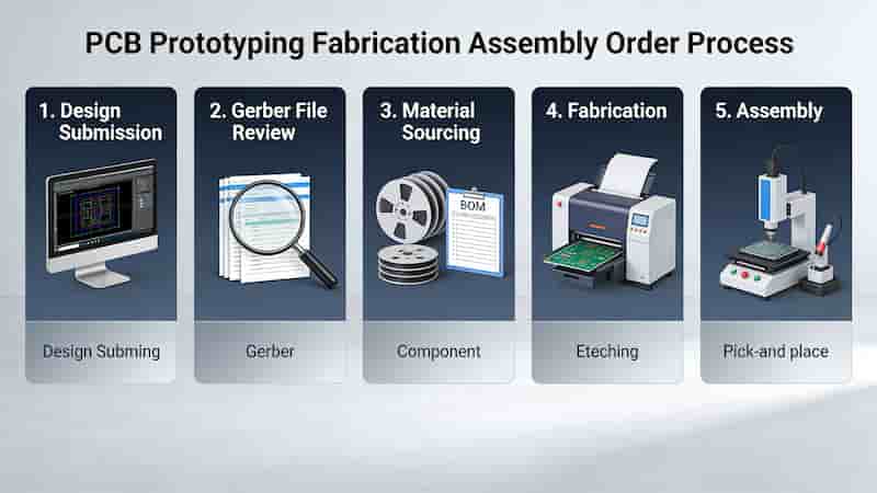
5 Simple Steps to Order PCB Services
A streamlined process for PCB prototyping, fabrication, and turnkey PCBA projects for global buyers.
Ordering overseas PCB prototyping, fabrication, or assembly can feel complex for hardware teams and growing businesses. This guide supports engineers, EMS buyers, startups, and OEMs needing reliable small-batch or volume production with clear pricing, fast lead times, and professional engineering support.
Follow these steps to submit files, get a firm quote within 24 hours, and receive high-quality China-made PCBs or turnkey PCBA in 3-5 days for prototypes and 5-10 days for assembly. We keep the process transparent and risk-controlled from inquiry to delivery.
Step 1: Contact Us for PCB Consultation
Reach our team via email or WhatsApp to discuss project needs. Our engineers help you select the right manufacturing and assembly solution for your volume, lead time, and technical requirements.
Whether you need standalone PCB fabrication or full turnkey PCBA with component sourcing, we recommend the most practical option.
Step 2: Submit PCB Files & Specifications
Send Gerber files, BOM, CPL, drill files, and full specs: layer count, dimensions, thickness, copper weight, surface finish, solder mask, impedance control, or blind vias.
Our engineering team reviews incomplete files pre-quotation to reduce DFM risks and avoid production delays.
Step 3: Receive Fast, Clear Quotation
We review your files and send a detailed quote within 24 hours for standard PCB projects, with quick-turn options for urgent orders.
The quote confirms pricing, lead time, assembly options, and shipping methods so you can evaluate risks before ordering.
Step 4: Confirm Order & Secure Payment
Approve the quote, confirm your order, and pay securely via PayPal or wire transfer.
We support flexible low-volume orders starting at 1 piece for PCB prototyping, ideal for startups and R&D teams.
Step 5: Production, Inspection & Global Delivery
Production starts immediately after payment. Boards go through AOI, X-ray, electrical testing, and functional checks as needed.
Finished PCBs or PCBA are shipped worldwide with tracking. Typical lead times: 3-5 days for PCB prototyping, 5-10 days for PCB assembly.
Typical Prototype PCB Timeline
Day 1: Inquiry & File Review – Send Gerber files and project details; our team checks manufacturability.
Day 1: Quotation – Receive full quote with pricing, lead time, and shipping within 24 hours.
Day 2: Order Confirmation – Approve quote and pay; order released to production.
Day 3-5: PCB Fabrication – Manufacturing and strict quality control inspection.
Day 5-7: Shipping & Delivery – Worldwide courier with full tracking.
Need turnkey PCBA? Contact us for a combined PCB fabrication and assembly schedule.
Industry Applications We Support
We provide PCB prototyping, fabrication, and assembly for diverse industries from R&D to mass production.
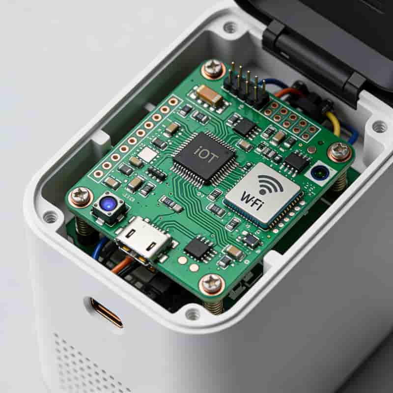
IoT & Smart Devices
High-density, small-form-factor PCBs with fast Prototype PCB Services turnaround for rapid product iteration.
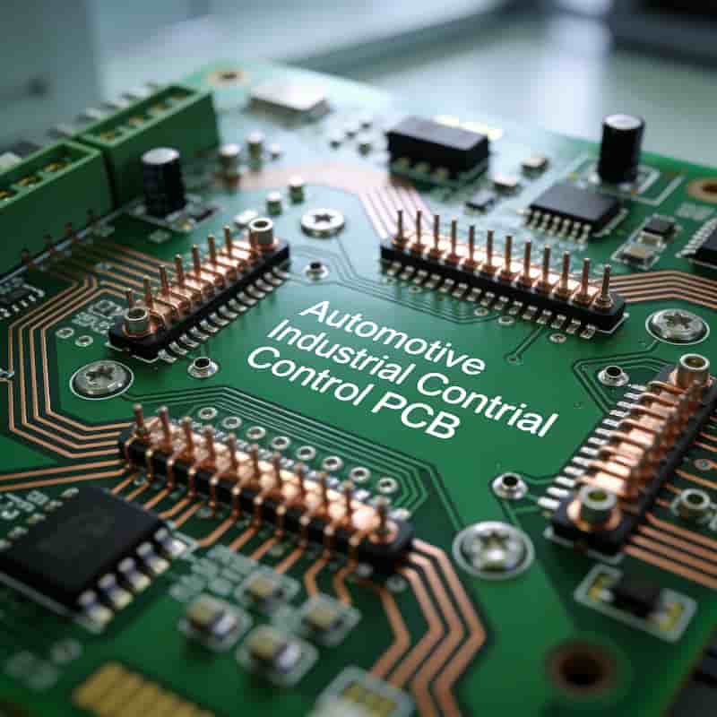
Automotive & Industrial Control
Multilayer high-reliability PCBs meeting IPC Class 2/3 for harsh environments.
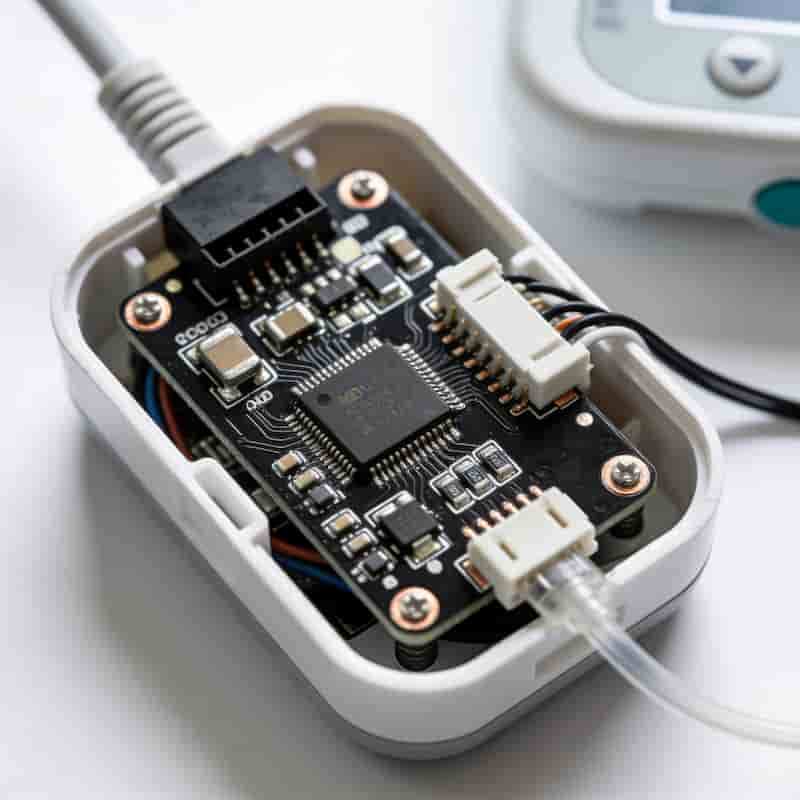
Medical & Health Electronics
Stable quality, traceability, and strict process control for prototype to low-volume production.
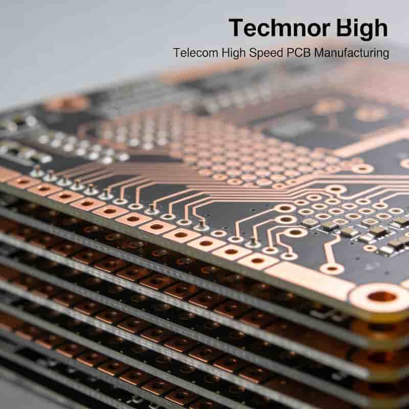
Telecom & High-Speed Design
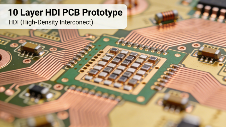
Impedance control, advanced materials, and Multilayer PCB Fabrication stack-ups for signal integrity.
Check capabilities: Technical Capabilities
Free PCB Quote Request
Submit your details to get a free quote for PCB prototyping and assembly within 24 hours.
What You Receive
- Free DFM review for your PCB design
- One-to-one engineering support
- Clear quote within 24 hours
- Support from 1-piece prototypes to volume production
Upload Gerber & BOM in ZIP/RAR (max 20MB each).
Tips for First-Time PCB Orders
These best practices speed up quoting, lower risks, and avoid delays for your PCB prototyping orders.
- Use clear file names and organized project packages
- Check drill files, board outlines, layers, and BOM before submission
- Provide complete specs early for accurate quoting
- Choose standard materials and finishes for cost-effective prototypes
- Request engineering feedback before final order confirmation
Start Your PCB Order Today
Get a free quote for PCB prototyping, fabrication, and assembly. Fast quotes, reliable quality, global delivery.
Request Free Quote Now
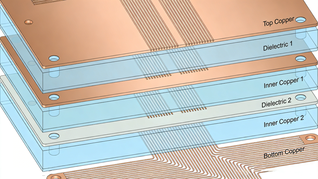
Multilayer Flexible PCB Manufacturer | Custom 4–16 Layer Flex Circuits
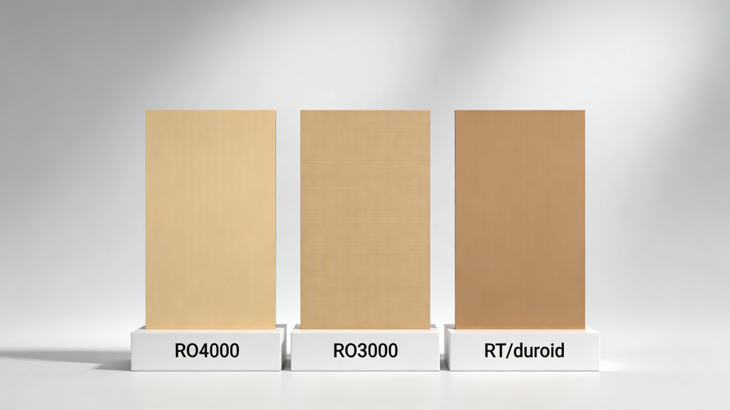
Rogers PCB: Full Guide to High-Frequency & High-Speed Circuit Boards
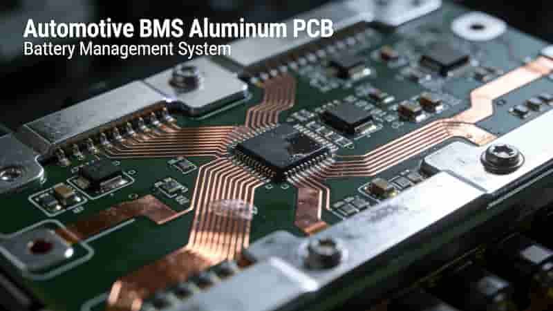
What Are Aluminum PCBs Used For? Applications and Benefits for Industrial Buyers
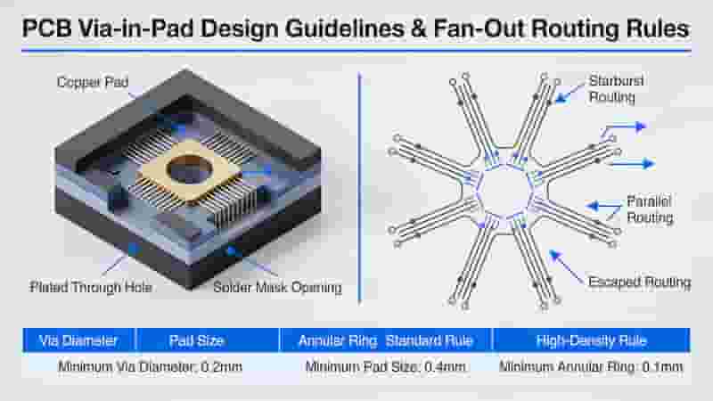
Via-In-Pad Design Guidelines and Manufacturing Process for PCB
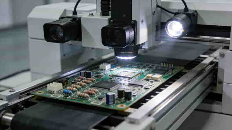
Surface Mount Technology (SMT) PCB Assembly Service