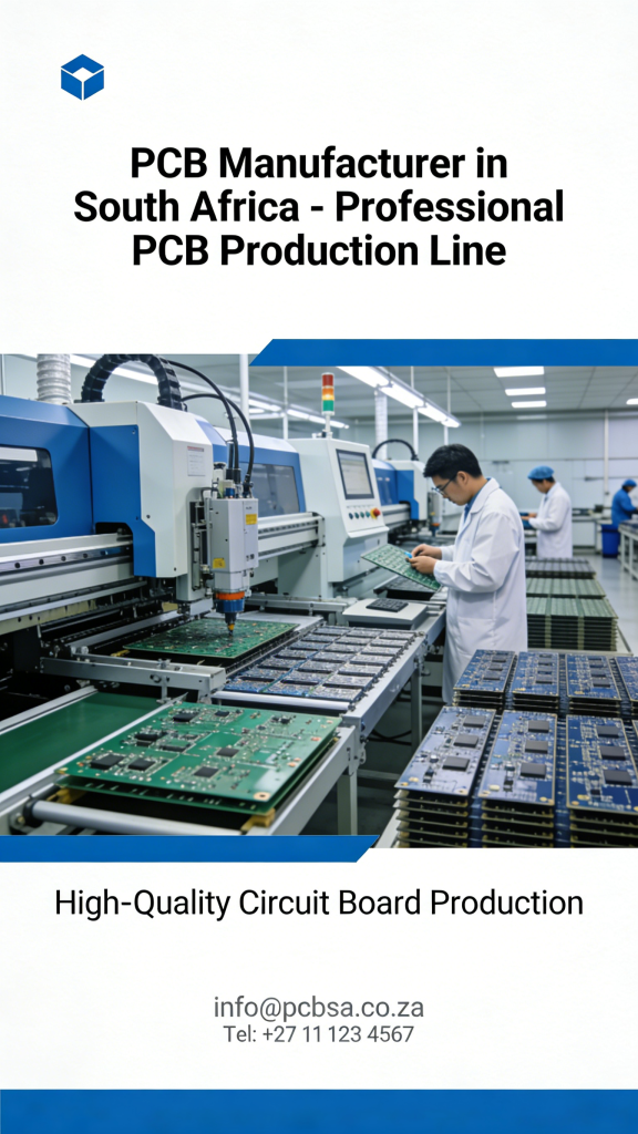
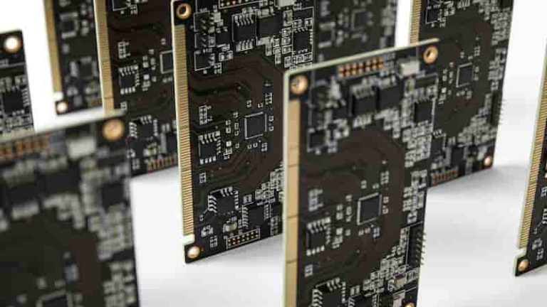
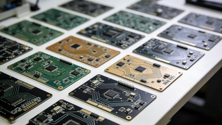
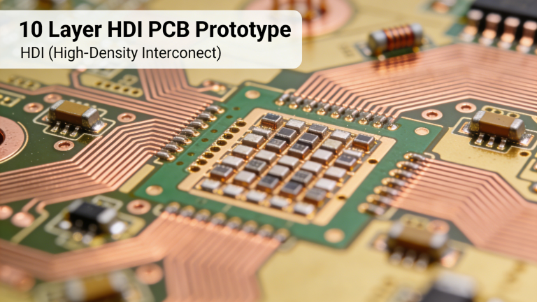
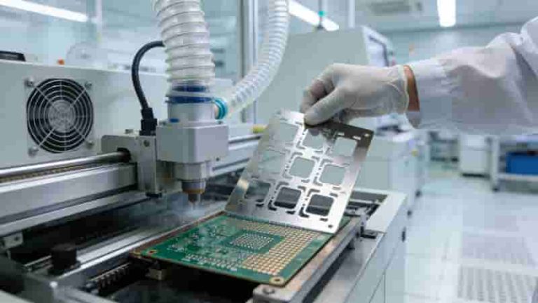
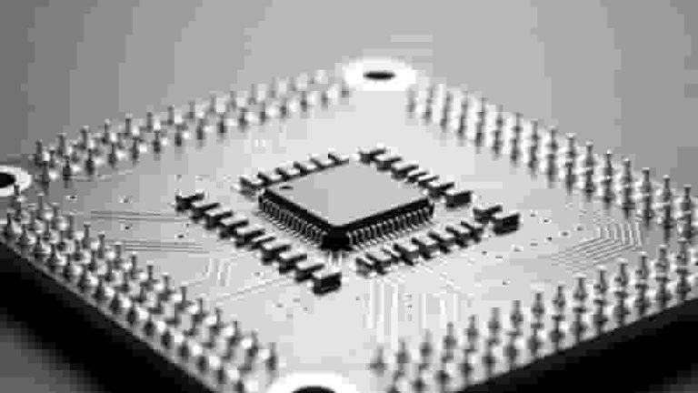
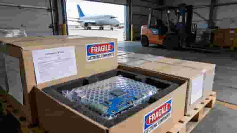
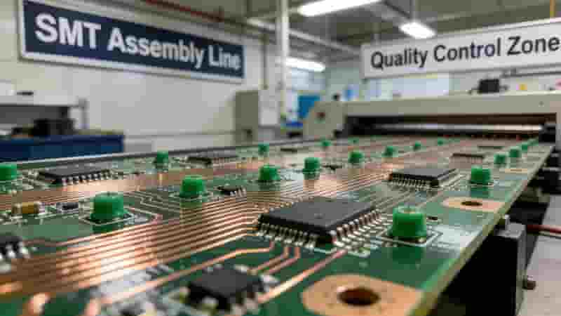
Surface Mount Technology (SMT) PCB Assembly Service mounts electrical components directly onto the surface of printed circuit boards without through-hole leads. As a leading assembly solution for modern electronics, it delivers compact size, high reliability, and cost efficiency for industrial, medical, automotive, and consumer products worldwide.
We provide one-stop service covering PCB production, component sourcing, and full turnkey SMT PCB assembly to support your project from prototype to mass production.
What is SMT PCB Assembly?
Surface Mount Technology (SMT) is a modern PCB assembly method where components are mounted directly on the board surface. No drilling or through-hole leads are required. Components used are called Surface Mount Devices (SMD), with the smallest size as small as 0.6mm × 0.3mm.
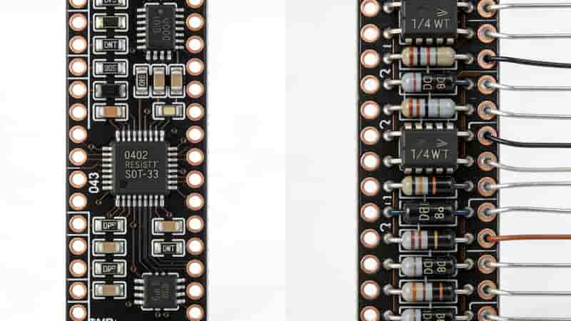
SMT enables higher circuit density, smaller product size, faster production, and better stability than traditional through-hole assembly. It has become the dominant assembly technology in the global electronics industry.
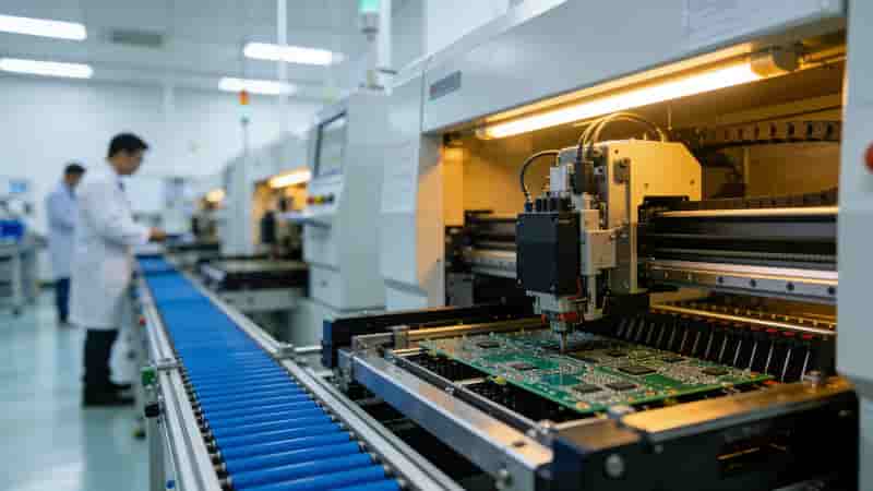
Our SMT Assembly Capabilities
We operate fully automatic high-speed SMT PCB assembly lines equipped with industry-leading equipment to support precision assembly for global customers.
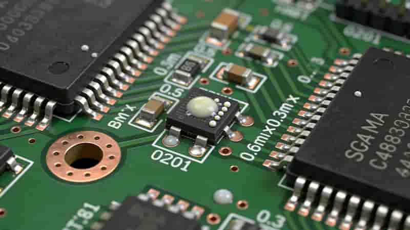
- Component range: 01005, 0201, 0402, BGA, μBGA, QFN, LGA, PoP
- Fine pitch capability: 0.25mm pitch components
- Board types: rigid, flex, rigid-flex, metal core, HDI
- Assembly types: single-sided, double-sided, mixed SMT+THT
- Volume: prototype to mass production, no MOQ
- Quality standard: IPC Class 2, IPC Class 3
- Capacity: 5 million SMT points/day, 50–100 models/day
- Free DFM/DFA analysis
SMT vs Through-Hole Assembly (THT)
Understanding the difference helps you select the right assembly solution for your product.
| Item | SMT Assembly | Through-Hole (THT) |
|---|---|---|
| Component Size | Ultra-small, miniaturized | Larger, leaded |
| Board Density | High density, compact design | Low density, larger board |
| Production Speed | Fast, fully automated | Slow, more manual work |
| Shock/ Vibration Resistance | Excellent | Good for high stress |
| Best For | Consumer, industrial, medical | High-power, high-voltage parts |
Full SMT PCB Assembly Process
Our standardized SMT PCB assembly process ensures stable quality and on-time delivery for every order.
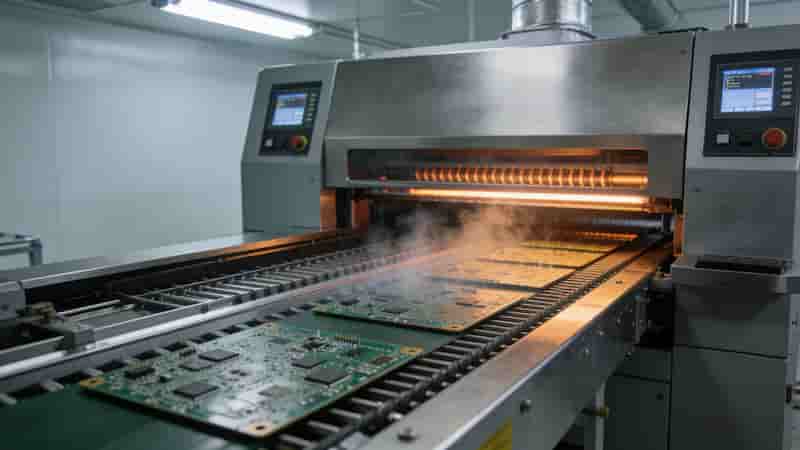
- PCB Design & File Preparation: Gerber, BOM, pick-and-place files
- DFM Check: Free design optimization to avoid production risks
- Component Sourcing: Authentic components with full traceability
- Solder Paste Printing: Precise printing via laser-cut stencil
- Pick & Place: High-speed automatic component placement
- Reflow Soldering: Multi-zone temperature control soldering
- Inspection & Testing: AOI, X-ray, ICT, functional test
- Packaging & Shipment: Anti-static packaging for global delivery
Testing & Inspection Capabilities
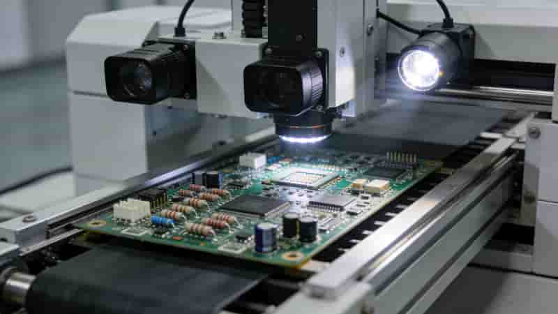
We enforce full inspection throughout SMT PCB assembly to guarantee zero-defect quality.
- Solder Paste Inspection (SPI)
- Automatic Optical Inspection (AOI)
- X-ray Inspection for BGA/QFN
- First Article Inspection (FAI)
- In-Circuit Test (ICT)
- Functional Performance Test
Industry Applications
Our SMT PCB assembly serves high-reliability markets worldwide:
- Aerospace & Defense
- Medical Devices
- Automotive Electronics
- Telecommunication Equipment
- Consumer Electronics
- Industrial Control & IoT
- LED Lighting & Display
Frequently Asked Questions
1. What files do you need for an SMT assembly quote?
We require Gerber files, BOM list, and pick-and-place files for accurate evaluation.
2. Do you support BGA and fine-pitch assembly?
Yes. We assemble BGA, QFN, μBGA, and components down to 0.25mm pitch.
3. Do you provide lead-free assembly?
We support both leaded and RoHS-compliant lead-free SMT PCB assembly.
4. What is your typical lead time?
Prototype orders: 3–7 days; mass production: 7–15 days based on quantity.
5. Is there a minimum order quantity?
No MOQ. We accept prototype, small-batch, and mass production orders.
Why Choose Our SMT PCB Assembly Service?
- One-stop turnkey solution: PCB + components + assembly + test
- Advanced equipment and strict IPC quality standards
- Free DFM/DFA to reduce risks and cost
- Flexible order volume, fast turnaround
- ISO, RoHS, UL certified process
- Global logistics and responsive support
Request a Quote & Start Your Project
Get professional SMT PCB assembly with high quality, fast lead times, and competitive pricing. Send us your Gerber files and BOM for a free, no-obligation quote today.
Get Free SMT Assembly Quote
Single Layer PCB Manufacturing | Affordable Single Sided PCBs
Understanding Plated Through Holes (PTH) for Printed Circuit Boards
What is a PCB BOM and How to Create One
PCB Design Guidelines for Manufacturing & IPC Compliance
What Are Tented Vias? A Complete PCB Design Guide