PCB Prototype Manufacturing in China: Benefits, Challenges & Reliable Solutions
PCB prototype manufacturing in China delivers exceptional cost efficiency, fast lead times, advanced engineering capabilities, and scalable production for global electronics buyers. This guide breaks down key advantages, common risks, and how to secure consistent quality for your prototype projects.
Introduction to PCB Prototype Manufacturing in China
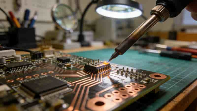
Printed Circuit Boards (PCBs) are the core of modern electronic products, and PCB prototyping is a critical step in product development, testing, and mass production preparation. China has become the global center for PCB prototype manufacturing due to its complete industrial chain, cost advantages, technical maturity, and fast response capabilities.
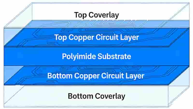
We focus on providing stable, high-precision PCB prototype services for international engineers, procurement teams, and OEM/ODM clients, supporting single-sided, double-sided, multi-layer, HDI, rigid, flex, and rigid-flex PCB prototypes.
Key Advantages of China PCB Prototyping
Cost Efficiency
China offers competitive labor costs, large-scale raw material supply, and optimized production processes, greatly reducing the cost of PCB prototype manufacturing without sacrificing quality. Lower overhead and material expenses bring direct budget benefits to global buyers.
Skilled Engineering Workforce
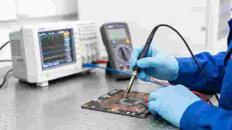
A large number of electronics technicians and PCB engineers ensure precise handling of DFM review, prototype fabrication, testing, and optimization. Professional teams support complex PCB designs and high-demand prototype projects.
Advanced Technology & Equipment
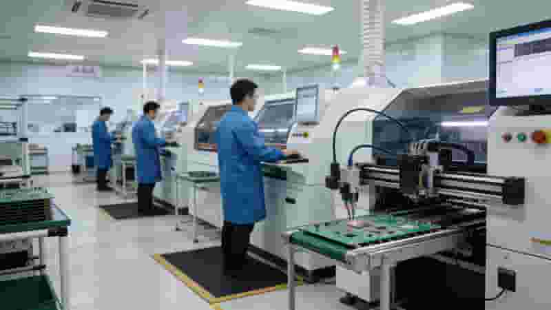
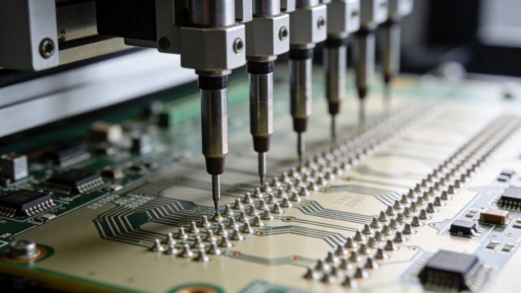
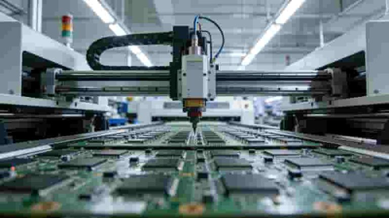
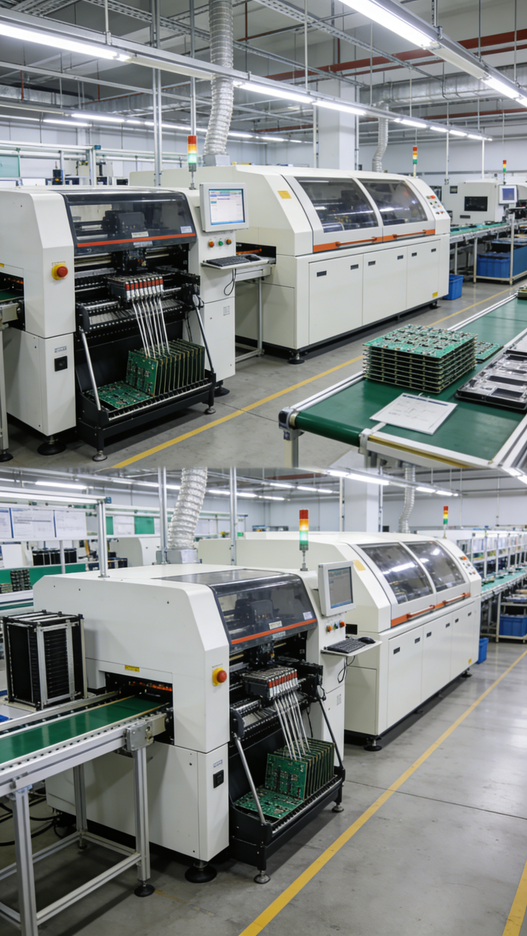
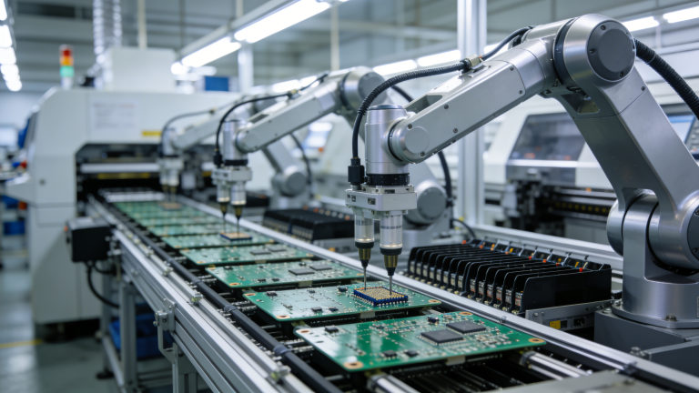
Chinese PCB factories use advanced laser plotting, electroplating, etching, lamination, and automated testing equipment. Continuous technical upgrades support high-density, high-precision, and high-frequency PCB prototypes for industrial, medical, automotive, and consumer electronics.
Fast Turnaround & Supply Chain Integration
Complete upstream and downstream supply chains shorten material preparation and production cycles. Many reliable manufacturers support rapid prototype delivery, helping clients accelerate product launches and market testing.
How to Select a Reliable PCB Prototype Manufacturer in China
Choosing a trusted partner directly determines prototype quality, delivery stability, and project security. Here are the key criteria:
Complete certifications: ISO 9001, IPC-A-600, UL, etc.
Strict quality control and full-process testing
Clear English communication and professional technical support
Stable supply chain and on-time delivery record
Strong IP protection policies and practices
Challenges of China PCB Prototype Manufacturing & Solutions
Quality Control Risks
Some small manufacturers lack standardized processes, leading to inconsistent quality. We eliminate this risk through incoming material inspection, production monitoring, and finished product functional testing to ensure each PCB prototype meets specifications.
Intellectual Property Protection
IP security is a top concern for global buyers. We implement strict non-disclosure agreements (NDAs), encrypted file management, and limited access to design data to fully protect client IP.
Communication & Cultural Barriers
Professional English-speaking account managers and engineers provide clear, timely communication throughout DFM, production, and after-sales support to avoid misunderstandings.
Supply Chain & Logistics Risks
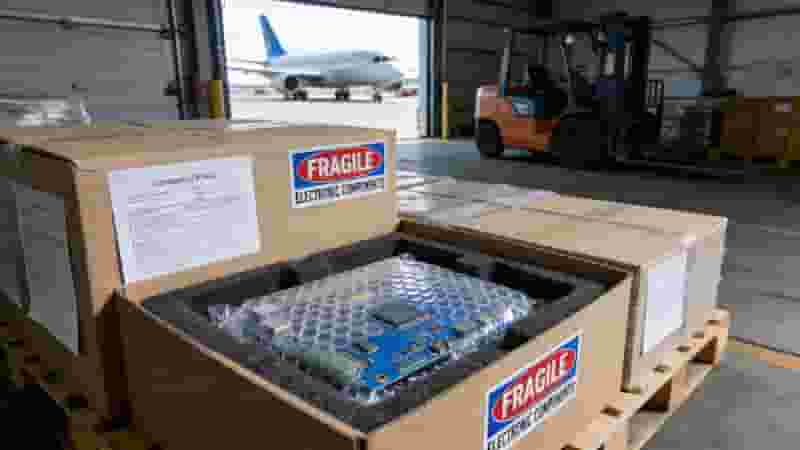
Stable long-term material suppliers and mature international logistics systems ensure on-time delivery and reduce delays caused by supply chain fluctuations.
China PCB Prototyping Comparison
Item
Standard Suppliers
Our Professional Service
Quality Stability
Inconsistent
ISO & IPC Certified
Lead Time
Uncertain
Fast & On-Time
IP Protection
Weak
Strict NDA & Security
Communication
Limited
Professional English Support
Why Choose Us for Your PCB Prototypes
We integrate the full advantages of PCB prototype manufacturing in China with strict quality management and customer‑centric services. Our core capabilities include:
Full-range prototype PCB fabrication and assembly
DFM analysis and design optimization
Rigorous electrical and performance testing
Flexible order quantities from samples to small batches
Global delivery with reliable logistics
Conclusion
PCB prototype manufacturing in China provides outstanding value in cost, technology, speed, and scalability for global electronics projects. The key to success is selecting a professional, reliable, and secure manufacturing partner.
We focus on delivering high-quality, on-time PCB prototype services that meet international standards, helping you turn designs into validated products efficiently.
Start Your PCB Prototype Project Today
Get a free quote, DFM check, and custom solution for your PCB prototype needs. Contact us now to accelerate your product development.
HDI PCB is an advanced printed circuit board technology for high‑component‑density electronics. This guide covers core HDI PCB layout principles, via design, trace rules, stackup, and IPC standards for engineers and buyers. What Is HDI PCB Layout? High Density Interconnects (HDI PCB) layout refers to advanced PCB design techniques used when trace widths drop below…
Learn industrial-grade methods to safely and accurately detect PCB short circuits using visual inspection, multimeters, thermal imaging, and X-ray, compliant with IPC standards for electronics manufacturing and repair. Understanding PCB Short Circuits The distinctive burnt smell from faulty electronics often signals a PCB short circuit. This occurs when current flows along an unintended path, causing…
Selecting a trusted PCB prototype manufacturer directly impacts product performance, development speed, and long-term reliability. This professional guide helps engineers and buyers evaluate technical capabilities, quality systems, lead times, and services to pick the ideal partner for your electronic projects. Technical & Manufacturing Capabilities A professional PCB prototype manufacturer must match your design complexity and…
PCBs are the backbone of modern electronics. While Rigid PCB and Flex PCB serve similar core functions, they differ greatly in materials, flexibility, cost, durability, and ideal use cases. This professional guide helps engineers and buyers choose the right PCB for industrial and export projects. Printed Circuit Boards (PCBs) are the backbone of modern electronics,…
PCB Design Software Free Download This is a comparison of several PCB design tools that meet the following criteria: 1. PartSim PartSim is a free, user-friendly online circuit simulator featuring a full SPICE simulation engine, web-based schematic capture, a graphical waveform viewer, and direct Digi‑Key integration—all accessible via your web browser. It also includes an…
Understanding the key differences between PTH and via is essential for optimizing PCB design and manufacturing. This article defines PTH and via, compares dimensions, functions, locations and finishing requirements. Typical applications and design considerations are also discussed to help engineers and buyers make informed decisions. Defining PTH and Vias in PCBs PTHs (Plated Through Holes)…
We specialize in LED PCB manufacturing and assembly with aluminum, copper & flexible substrates featuring superior heat dissipation. ISO 9001 certified, fast turnaround & competitive pricing for global LED lighting projects. Superior Heat Dissipation 1-9 W/mK thermal conductivity Fast Turnaround 24-hour quote, 3-5 days delivery ISO 9001 Certified International quality standard One-Stop PCBA Service From…
OSP (Organic Solderability Preservative) is a lead‑free, water‑based organic coating applied to exposed copper pads on printed circuit boards to prevent oxidation and ensure reliable soldering for SMT assembly. This complete guide covers definition, process, pros & cons, comparisons, storage, assembly best practices, and ideal applications for global engineers and buyers. What Is PCB Surface…
Double-sided flex PCB (also known as 2-layer flexible PCB) is a flexible circuit with two copper conductive layers on polyimide film, connected by plated through holes. We provide full-process manufacturing, customized stackup, strict quality control and fast delivery for global industrial, medical, automotive and high-tech electronics applications from prototype to mass production. What Is a…
Flying Probe Testing for PCB is a fixtureless electrical test method ideal for low-volume production and prototype circuit boards. Top EMS providers and PCB assembly manufacturers use this advanced technology to ensure high-quality products. Complex PCB circuits often have hidden defects such as short circuits, open circuits, diode faults, and bad solder connections. These issues…
PCB stackup design directly determines signal integrity, EMI control, power stability and manufacturing reliability. This guideline provides professional, field-proven best practices for 2‑layer PCB stackup, 4‑layer PCB stackup and 6‑layer PCB stackup for industrial electronics, communications equipment and high‑speed digital products. Introduction to PCB Stackup Design PCB stackup design is the foundation of high‑performance printed…
HASL (Hot Air Solder Leveling) is one of the most widely used and cost‑effective PCB surface finish processes in electronics manufacturing. It provides excellent solderability, protects copper from oxidation, and supports reliable assembly for through‑hole and standard SMT applications. This guide explains the HASL process, benefits, limitations, lead‑free options, and comparisons to help you select…
A Surface Mount Device (SMD) component package is a standardized enclosure designed for direct soldering onto PCB surfaces, enabling high-density assembly, miniaturization, and automated manufacturing in modern electronics. What Is an SMD Component Package? SMD stands for Surface Mount Device, referring to electronic components designed exclusively for Surface Mount Technology (SMT) assembly. An SMD component…
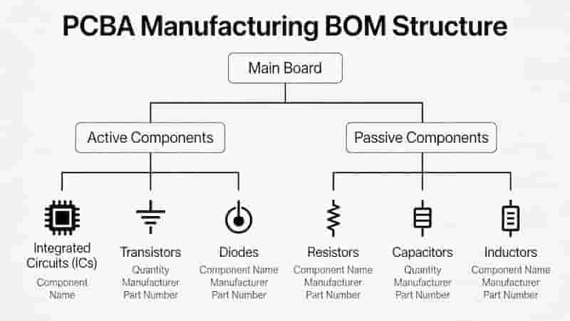
Discover how a PCB BOM streamlines PCBA manufacturing. Our guide offers expert tips and tools for error-free PCB assembly, accurate sourcing, cost control, and on-time production for industrial buyers, engineers, and procurement teams. Imagine heading to the grocery store with a detailed shopping list to ensure you get everything you need, organized and error-free. In…
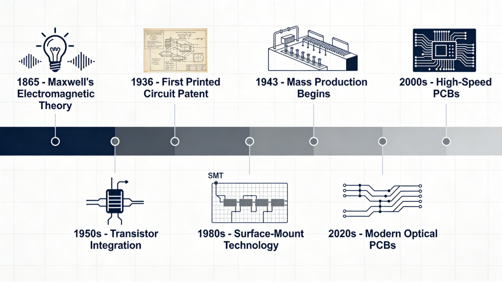
Explore the complete evolution of printed circuit boards from early electromagnetic theory to modern HDI, flexible, and optical PCBs. This timeline covers key inventions, military adoption, mass commercialization, and future trends for global electronics manufacturing. PCB Prehistoric Era & Electromagnetic Foundations The journey of printed circuit boards starts with the discovery of electromagnetic principles that…
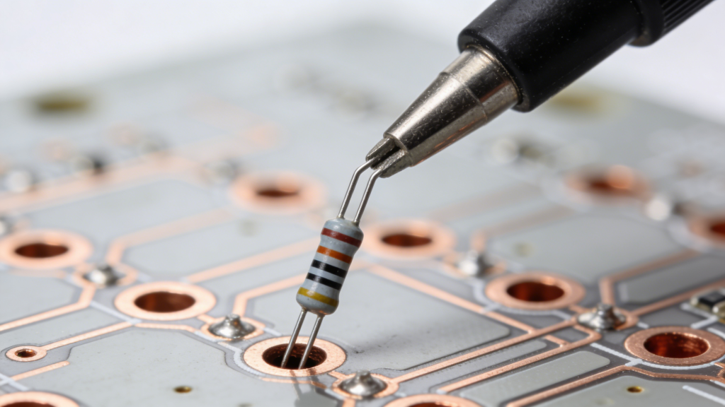
We provide reliable through-hole PCBAs assembly service for industrial, power, medical, aerospace and automotive applications. Our IPC-standard THT assembly supports prototypes to mass production with wave soldering, selective soldering and full inspection. Through-hole PCB Assembly Service Overview Our through-hole PCB assembly fulfills leaded assembly demands across industries. We deliver single-sided, double-sided and high-density multilayer through-hole…
This guide details all essential PCB & PCBA manufacturing files, including Gerber files, BOM lists, NC Drill files, Centroid files, and other critical documents. It provides professional standards, format requirements, and technical parameters to ensure accurate quotes, error-free production, and reliable PCB assembly for global industrial buyers, engineers, and procurement teams. Core Files for PCB…
FR-4 is the most widely used flame-retardant glass-epoxy laminate material for rigid PCB manufacturing. Defined by NEMA standards, it offers excellent electrical insulation, mechanical strength, thermal stability, and cost efficiency, making it the global industry standard for most electronic applications. What is FR-4 Material? FR-4 (Flame Retardant Grade 4) is a NEMA-defined material grade for…
Microvias are core interconnect structures that drive PCB miniaturization and high‑density design. This professional guide covers definitions, types, fabrication, reliability, applications and how we deliver high‑quality microvia PCB solutions for global industrial buyers. What Are Microvias in PCBs As printed circuit boards integrate more components into smaller spaces, microvias become essential for advanced PCB miniaturization….
This professional guide covers HDI PCB layout practices, stack-up, microvias, routing rules, DFM, impedance control and IPC standards to help engineers and procurement teams build reliable, mass-producible HDI PCB for high-speed, miniaturized electronics. What Is HDI PCB Layout HDI PCB (High-Density Interconnect) layout refers to design methods used when trace widths drop below 8 mils…
A flexible PCB (FPC) is a thin, bendable printed circuit that can fold, twist, and fit compact 3D spaces. This guide covers structure, materials, stack‑ups, design rules, manufacturing, and real‑world use cases to help global engineers and buyers select the right flex solution. Introduction In every new generation of electronic products, there is a clear…
IPC standards are the global industry benchmarks governing PCB design, fabrication, assembly, inspection, testing, and documentation. This guide covers core IPC standards, compliance classes, technical specifications, and how adherence ensures reliability, consistency, and market acceptance for industrial, automotive, medical, and aerospace electronics. What Are IPC Standards IPC (Association Connecting Electronics Industries) is the global governing…
FAQs About PCB Prototype Manufacturing in China
A: It features cost competitiveness, mature technical capabilities, advanced production equipment, complete industrial chains and fast delivery to speed up product development.
A: They support single-sided, double-sided, multilayer, HDI, rigid, flexible and rigid-flex PCB prototypes for diverse application demands.
A: Qualified manufacturers shall have ISO 9001, IPC-A-600, UL and other internationally recognized quality certifications.
A: Main risks include unstable quality, IP leakage, communication gaps and potential logistics delays.
A: Sign formal NDAs, adopt encrypted file management and restrict data access to prevent unauthorized use or disclosure.
A: Work with suppliers equipped with professional English-speaking teams to ensure smooth communication on DFM, production and after-sales issues.
A: Verify valid certifications, full-process quality control, IP protection rules, communication ability and on-time delivery records.
A: Yes. Most professional manufacturers support flexible orders from samples to small batches and seamless production transition.
Low-volume or small-batch PCB assembly is your best solution for flexible assembly parts on a relatively small batch of bare PCB boards! A low-cost PCB prototype is essential if you are looking at a new launch. After all, you do not want a situation where you deal with errors after a high-volume or mass production run. Alternatively, you could be…
Fast Prototype PCB Manufacturing Services in Canada provide rapid, high‑reliability printed circuit board prototyping for engineers, procurement teams, and OEMs across Canada. We offer quick‑turn rigid, flexible, rigid‑flex, HDI, and high‑frequency PCBs with IPC Class 2/3 standards, DFM support, 48–72 hour lead times, and seamless scaling to volume production. Core Prototyping Capabilities Our fast prototype…
Rapid PCB prototyping delivers fast-turn fabrication from 8 hours for double-sided boards to 24–72 hours for multilayer prototypes. We provide high-quality, IPC Class 2, RoHS & UL certified services to accelerate your product development. Why Choose Our Rapid PCB Prototyping In the fast-paced electronics industry, speed and quality are critical. We specialize in professional rapid…
As a trusted low-cost PCB assembly service provider, we deliver high-quality, affordable PCB assembly for prototypes, low-volume and mass production, with no hidden costs and global shipping. Why Low-Cost PCB Assembly Is Essential Printed circuit boards are the backbone of modern electronics, connecting components to deliver functional devices. With growing demand, more PCB assembly service…
Choosing a reliable quick turn PCB assembly manufacturer is critical when deadlines are tight and designs change fast. This guide explains what a quick turn PCB assembly manufacturer does, when you need one, key evaluation factors, and how a trusted China‑based partner helps you deliver high‑quality prototypes and low‑volume runs on time and within budget….
In today’s competitive electronics manufacturing landscape, understanding PCB assembly cost is critical for engineering and procurement teams. This guide breaks down all pricing factors, assembly types, volume impacts, and practical strategies to optimize your budget without sacrificing quality. What Is PCB Assembly? PCB assembly (PCBA) is the process of mounting electronic components onto a bare…