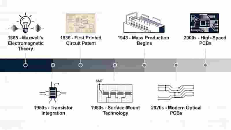
Explore the complete evolution of printed circuit boards from early electromagnetic theory to modern HDI, flexible, and optical PCBs. This timeline covers key inventions, military adoption, mass commercialization, and future trends for global electronics manufacturing.
PCB Prehistoric Era & Electromagnetic Foundations
The journey of printed circuit boards starts with the discovery of electromagnetic principles that shaped modern electronics. In 1831, Michael Faraday established electromagnetic induction, laying groundwork for electrical engineering.
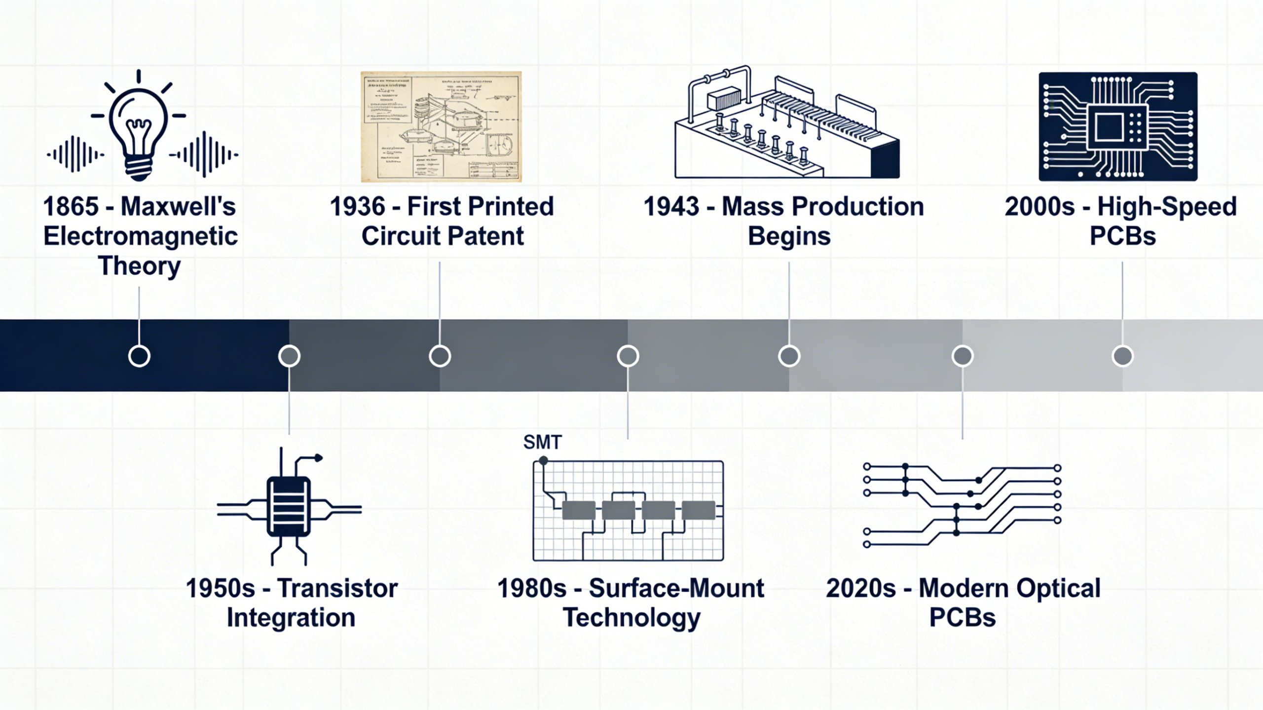
In 1864, James Clerk Maxwell published his electromagnetic field theory, predicting electromagnetic waves and unifying electricity, magnetism, and light. This framework became the theoretical foundation for all electronic interconnection systems, including PCBs.
Key milestones include the Edison Effect (1883), Hertz’s electromagnetic wave verification (1887), and the invention of vacuum tubes starting in 1897. These innovations created the need for reliable component interconnection—directly driving the creation of printed circuit boards.
Birth & Early Invention of Printed Circuit Boards
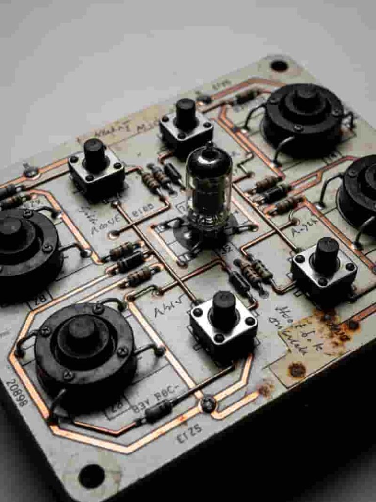
The first concept of printed circuits emerged in 1903 when German inventor Albert Hanson patented a flat foil conductor laminated structure—the earliest prototype of the printed circuit board.
In 1925, Charles Ducas successfully printed conductive patterns on insulating substrates. The modern PCB era began in 1936 when Dr. Paul Eisler invented the practical printed circuit method in the UK, earning him the title “Father of Printed Circuits.”
During WWII (1943), the US military adopted printed circuit boards for proximity fuzes and military radios, proving reliability in extreme conditions. Commercialization began in 1948.
Industrial Growth & Mass Adoption (1950s–1990s)
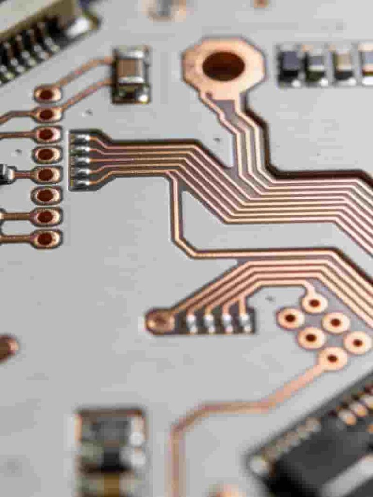
The invention of the transistor (1947) revolutionized electronics and accelerated printed circuit board adoption. Single-sided PCBs entered mass production in the 1950s using etching technology.
Double-sided PCBs with plated through-holes arrived in 1953. Multilayer printed circuit boards emerged in the 1960s to support integrated circuits (ICs) invented in 1958.
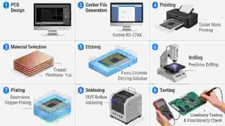
Surface Mount Technology (SMT) replaced through-hole mounting in the 1980s. CAD software automated PCB design, enabling faster prototyping and mass production.
| Period | PCB Type | Key Technology |
|---|---|---|
| 1903–1940s | Early Prototype PCB | Foil Lamination & Manual Etching |
| 1950s–1960s | Single & Double Sided | Plated Through-Hole (PTH) |
| 1970s–1990s | Multilayer PCB | SMT & CAD Design |
Modern PCB Technologies & HDI Development
Since the 1990s, printed circuit boards have evolved toward high density, miniaturization, and flexibility. BGA packaging and HDI (High-Density Interconnect) PCBs arrived in the mid-1990s.
HDI PCBs with microvias and any-layer interconnection (ELIC) enabled smartphone and portable device design. The mSAP and amSAP processes improved precision for fine-line printed circuit board manufacturing.
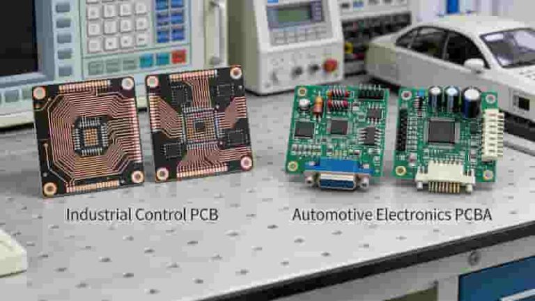
Flexible PCBs (FPC) and rigid-flex PCBs expanded use cases in wearables, automotive, and aerospace electronics.
Future Outlook of Printed Circuit Boards
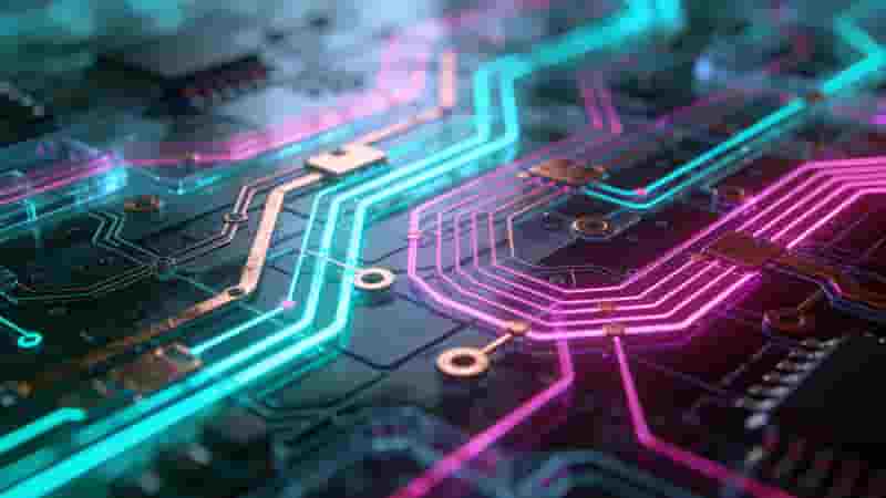
The future of printed circuit boards focuses on ultra-high density, optical interconnection, high-frequency materials, and sustainable manufacturing.
Optical PCBs will replace traditional copper interconnects to support 5G/6G, high-speed computing, and data centers. Embedded components, 3D stacking, and AI-driven design will further optimize PCB performance.
Environmental regulations will drive lead-free, halogen-free, and recyclable printed circuit board materials for global compliance.
Summary
From early electromagnetic theory to today’s advanced HDI and flexible designs, printed circuit boards have been the backbone of the electronics industry for over a century. PCBs enable miniaturization, reliability, and mass production for consumer, industrial, automotive, aerospace, and military applications.
As technology advances, printed circuit boards will continue evolving to meet demands for higher speed, smaller size, and greater functionality in the global digital economy.
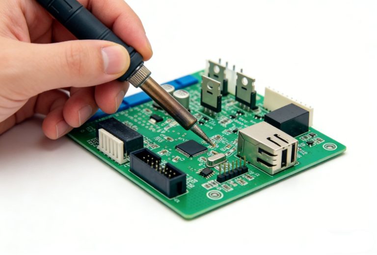
Custom Printed Circuit Board Solutions for Your Business
We provide professional PCB manufacturing, prototyping, and custom solutions for global buyers. Get a free quote now!
Inquire Now | Custom PCB Quote
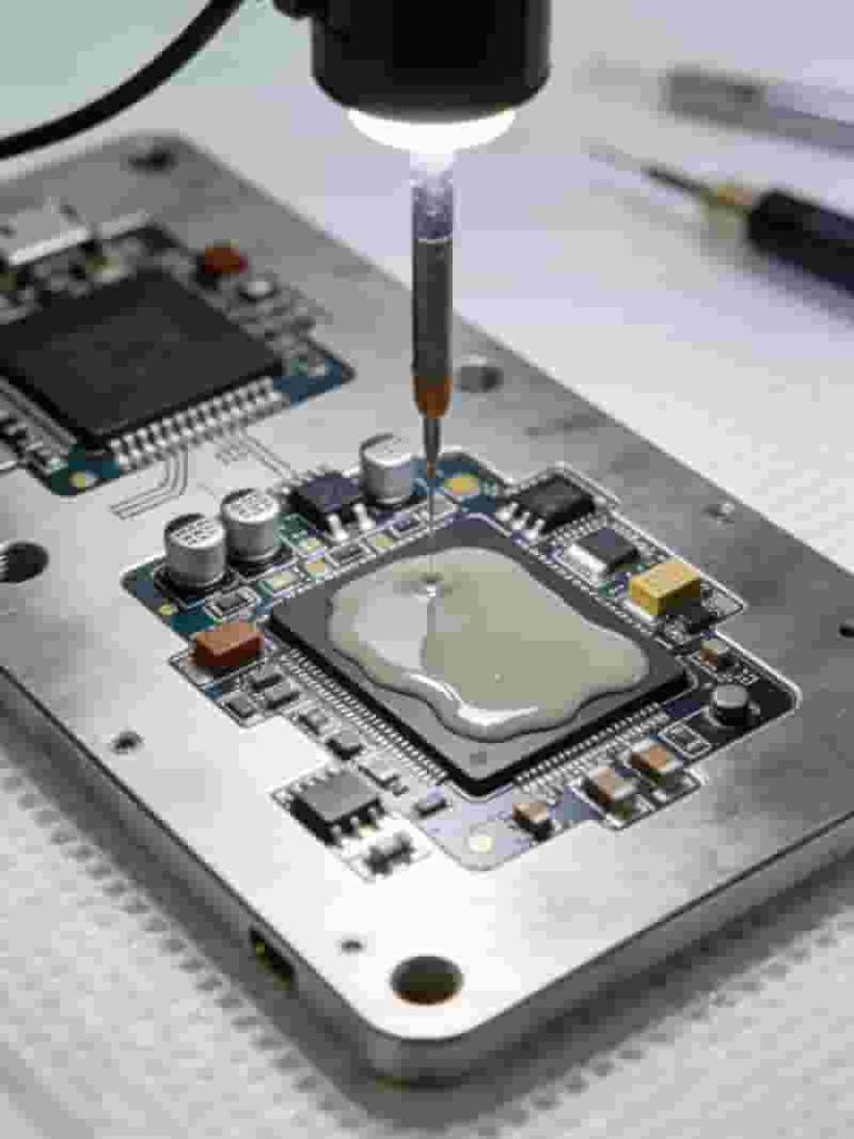
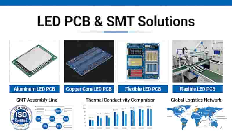
Aluminum PCB Manufacturing & Assembly Services
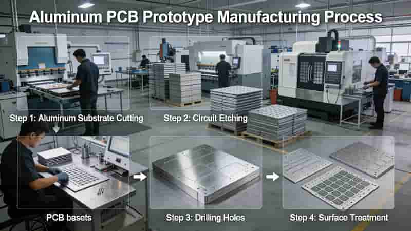
Aluminum PCB Prototype: The Ultimate Guide for Engineers and Designers
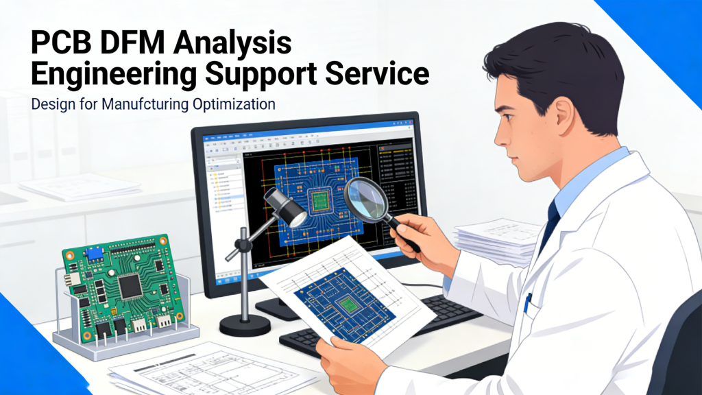
How to Choose the Right PCB Manufacturer and Supplier: Full Professional Guide
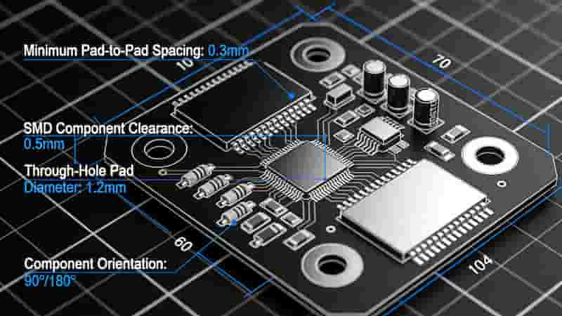
PCB Pad Design Basics: Standards, Rules & Best Practices for Engineers
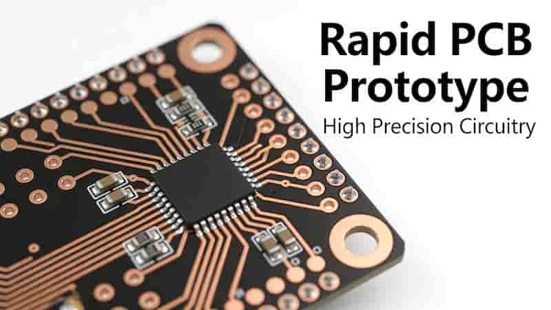
Accelerate Your Innovation with Rapid PCB Prototyping