|

Understanding Plated Through Holes (PTH) for Printed Circuit Boards 

Plated Through Hole PTH structure cross section for multilayer PCB

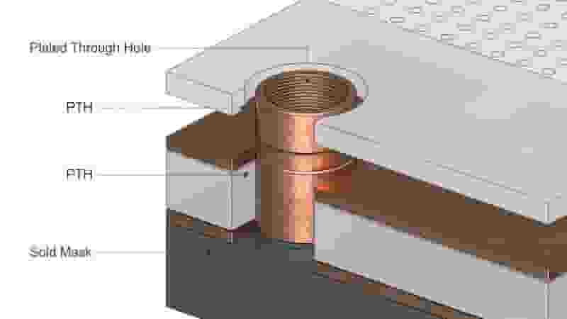
Plated Through Holes (PTH) are essential conductive structures in printed circuit boards that ensure stable interlayer connections, reliable component mounting, and long‑term performance. This guide explains PTH basics, design rules, manufacturing, comparisons to NPTH, blind vias, buried vias, and best practices for industrial PCB applications. 

Plated Through Hole PTH structure cross section for multilayer PCB

What Are Plated Through Holes (PTH) 

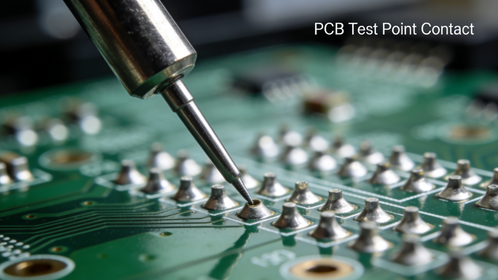
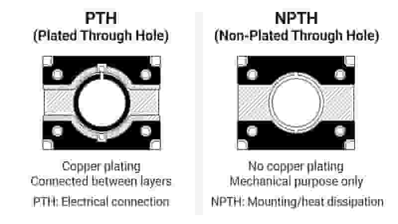
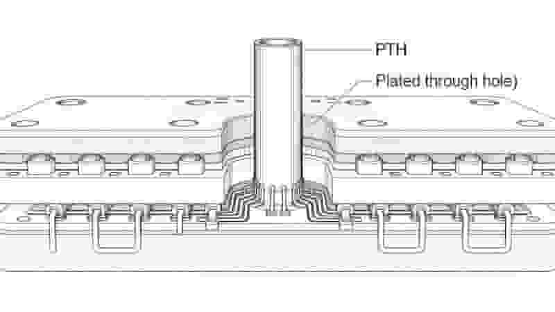
Plated Through Holes (PTH) are drilled holes in printed circuit boards with a conductive metal layer (usually copper) plated along the inner walls. These holes create permanent electrical connections between top, inner, and bottom layers of a PCB. 

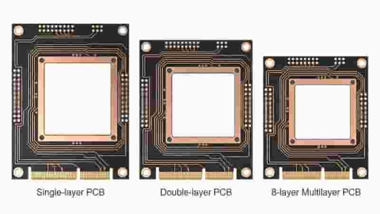
Unlike non‑plated holes, PTH provides continuous conductivity across the entire board thickness, making it essential for double‑sided and multilayer PCBs. 

Key Benefits of PTH in PCBs 

Reliable Interlayer ConnectivityPTH ensures stable signal transmission between layers even under vibration, temperature changes, and long‑term use. 

Dual‑Sided Component Placement – Components can be mounted on both sides of the board, maximizing space efficiency for compact designs.

Strong Mechanical Stability – Plated walls strengthen hole structure and improve solder joint reliability for through‑hole components.

High Current & Thermal Performance – Thick copper plating supports higher current loads and better heat dissipation.

PTH vs NPTH hole comparison for printed circuit board

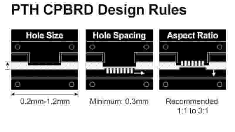
Critical PTH Design Considerations

Hole Size & Tolerance

Hole diameter must match component lead size. Standard PTH sizes range from 0.2 mm to 1.2 mm. Too small prevents insertion; too large weakens reliability.

Hole Spacing & Clearance

Spacing between PTH should be at least twice the finished hole diameter to avoid short circuits and plating defects.

Aspect Ratio & Depth

Higher aspect ratios (depth vs diameter) increase manufacturing difficulty and cost. Optimize PTH depth based on layer function.

Plating Thickness

Standard copper plating thickness for PTH is 20–25 μm for reliable conductivity and structural strength.

PTH PCB design rules hole size spacing aspect ratio

PTH vs Non‑Plated Through Holes (NPTH)

FeaturePTHNPTH
ConductivityFull interlayer connectionNo conductive layer
Use CaseMultilayer & double‑sided PCBMounting only, no conduction
ReliabilityHigh, industrial‑gradeLow, simple applications
CostModerateLower

Blind Vias, Buried Vias vs PTH

Blind Vias – Connect outer layer to inner layers but do not pass through the entire board. Save space and reduce drilling cost.

Buried Vias – Connect inner layers only, invisible from outside. Used in high‑density multilayer PCB.

PTH – Pass through full board thickness, simplest and most widely used for general interlayer connections.

PTH blind via buried via structure for PCB

Conclusion

Plated Through Holes (PTH) are foundational to reliable printed circuit board design. They deliver stable connectivity, mechanical strength, and design flexibility for industrial, automotive, medical, and consumer electronics.

By following proper design rules for size, spacing, and aspect ratio, you can maximize PTH performance while controlling production costs.

Need Professional PCB Manufacturing with PTH?

We specialize in high‑quality double‑sided and multilayer PCBs with precision PTH processing, strict quality control, and competitive pricing for global buyers.

Contact us for a free quote, design review, or custom PCB solution

Custom PCB Cost Overview 2025 Key Factors

Key Factors Influencing Custom PCB Costs in 2025

Posted on
0 Comments
Discover what drives custom PCB costs in 2025, from material choices and layer counts to board size and production volume. Compare area-based pricing for prototypes with detailed cost calculations for bulk orders. Unlock cost-saving strategies to balance quality and budget for your industrial & electronics projects. Introduction In 2025, custom PCBs continue to be the…
High Tg FR4 PCB layer structure and thermal stability diagram

Why FR4 Is the Preferred Material for High Tg PCBs: Benefits and Applications

Posted on
0 Comments
Summary: High Tg FR4 PCBs provide outstanding thermal stability, mechanical strength, electrical insulation, and cost efficiency for high-temperature electronics. This guide explains core properties, key benefits, industrial applications, and material comparisons to help engineers and purchasers select the right high Tg PCB solution for automotive, aerospace, industrial, and telecom systems. What Is a High Tg…
PCB prototyping process for design validation and testing

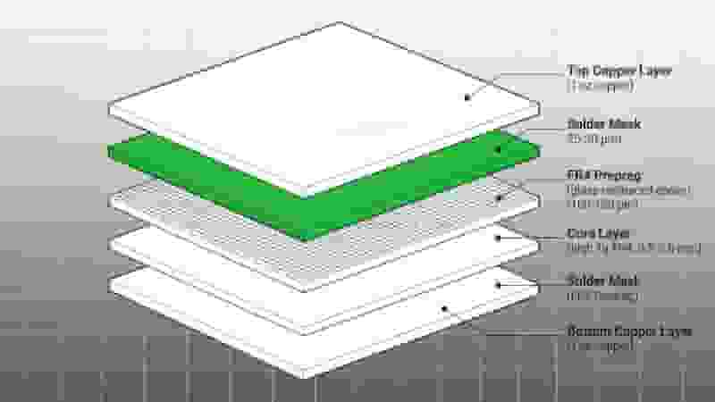
Accelerate Your Innovation with Rapid PCB Prototyping

Posted on
0 Comments
We provide professional Rapid PCB Prototyping with ultra‑fast lead times, strict quality control, and full customization for global engineers and buyers. From prototype to small‑batch production, we speed up your innovation and time‑to‑market. What Is Rapid PCB Prototyping Rapid PCB Prototyping is the fast production of small‑batch printed circuit boards to validate design, function, and…
PCB Solder Mask Cross Section Structure Diagram

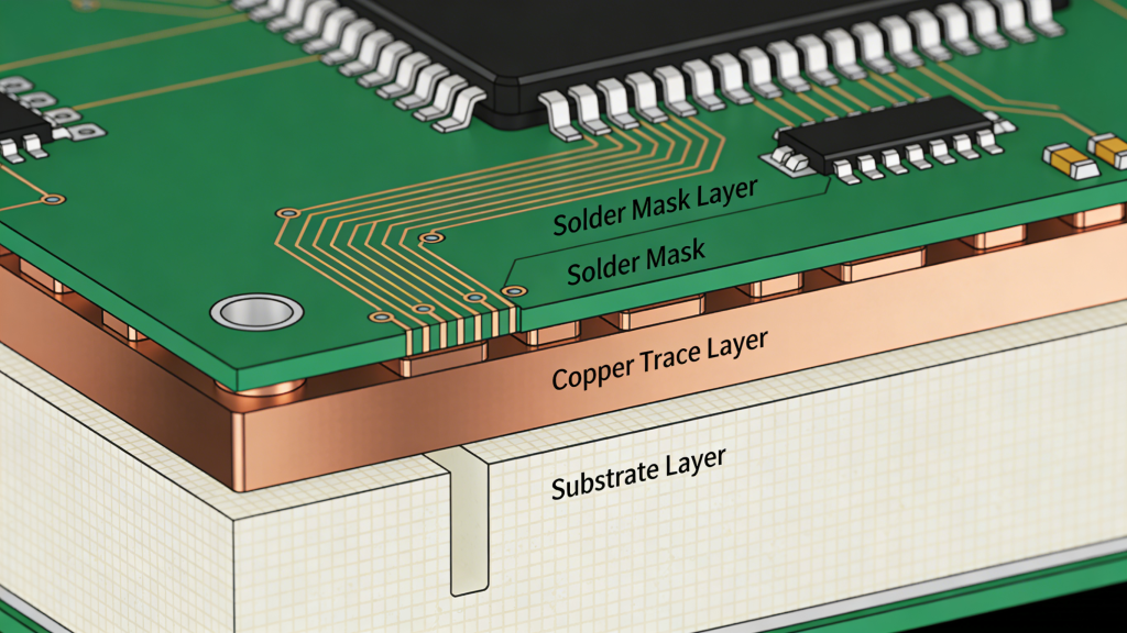
PCB Solder Mask: The Complete Professional Guide to Solder Resist Technology

Posted on
0 Comments
This guide covers everything about PCB solder mask (solder resist), including its functions, types, colors, application processes, thickness standards, IPC testing, and assembly compatibility. Learn how solder mask protects circuits, prevents solder bridging, and improves reliability for industrial and high-density PCBs. We explain how to select the right solder resist for rigid, flexible, and high-speed…
Fine-Pitch SMT PCB Assembly with BGA QFN Components

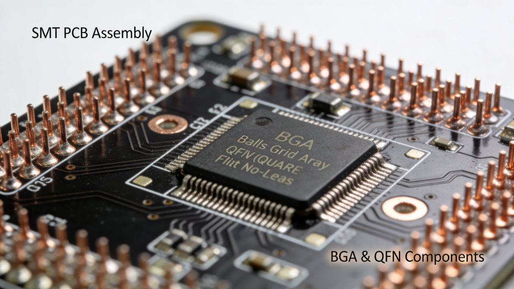
SMT PCB Assembly Services for Prototypes & Production

Posted on
0 Comments
We deliver reliable SMT PCB Assembly for rapid prototypes, NPI, low-volume and high-volume production. Our full turnkey solutions support fine-pitch components, BGAs, QFNs, rigid/flex‑rigid PCBs, and comply with IPC Class 2 & Class 3 standards for global industrial buyers. SMT PCB Assembly Capabilities We support full‑cycle SMT PCB Assembly from single prototypes to mass production,…
Advantages of Flying Probe Testing for PCB

Flying Probe Testing for PCB: The Complete Professional Guide

Posted on
0 Comments
Flying Probe Testing for PCB is a fixtureless electrical testing method widely used for prototype, low-volume and high-mix printed circuit board production. It accurately detects opens, shorts, wrong components, reverse polarity and soldering defects without expensive custom fixtures, making it the top choice for engineering verification and small-batch manufacturing. What is Flying Probe Testing? Flying…

FAQs About PCB PTH Definition, Design Spec & Comparison with NPTH/Blind Via

A: Full-board penetrating drilled hole with inner wall copper plating, realizing full-layer electrical conduction for through-hole component soldering and interlayer connection.

A: PTH with inner copper plating for electric conduction & component welding; NPTH bare hole only for mechanical fixation without any conductive function.

A: Common finished hole 0.2~1.2mm, hole diameter needs properly larger than component lead to guarantee smooth assembly and reliable soldering.

A: PTH runs through all layers; blind via links outer & partial inner layers; buried via totally hidden inside stackup connecting inner layers only.

A: Reasonable aspect ratio, enough hole spacing, matched pad size and standard 20~25μm inner copper plating thickness.

A: Excellent mechanical stability, support double-side component layout, high-current carrying capability and outstanding anti-vibration performance.

A: Fixed mounting hole without circuit connection requirement selects NPTH to cut plating cost for simple structural positioning.

A: Industrial control board, power supply PCB, traditional through-hole consumer product and low-to-medium layer count multilayer circuit.

Similar Posts