|

PCB Manufacturing Process Part 1: MI, Cutting & Drilling – Complete Industrial Guide

Copper Clad Laminate PCB Raw Material FR4 High Tg

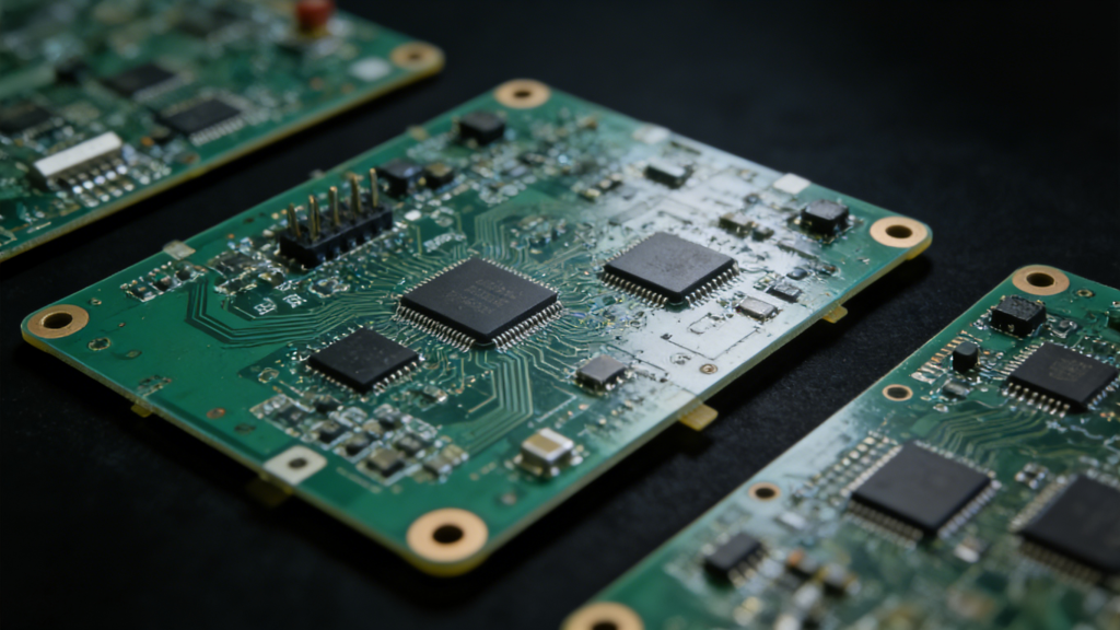
This professional guide covers the core initial stages of PCB manufacturing: Manufacturing Instruction (MI), material cutting, and precision drilling. Learn how industrial processes ensure accuracy, stability, and quality for reliable printed circuit boards.

Manufacturing Instruction (MI)

The Manufacturing Instruction (MI) is the most critical engineering document in PCB production. It converts Gerber and ODB++ files into standardized, repeatable manufacturing steps.

Our engineering team develops a complete MI file that defines layer structure, panel size, drill paths, material type, thickness, and quality standards. This document ensures every production step follows consistent rules.

PCB Manufacturing Instruction MI Document Gerber DFM

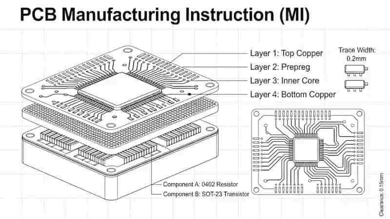
The MI file supports multi-project panelization to improve material utilization and lower unit cost while keeping high quality for global buyers.

PCB Material Cutting

Raw PCB copper clad laminates are supplied in large sheets: 49″×82″ and 49″×41″. These are automatically cut into standard production panels.

Copper Clad Laminate PCB Raw Material FR4 High Tg

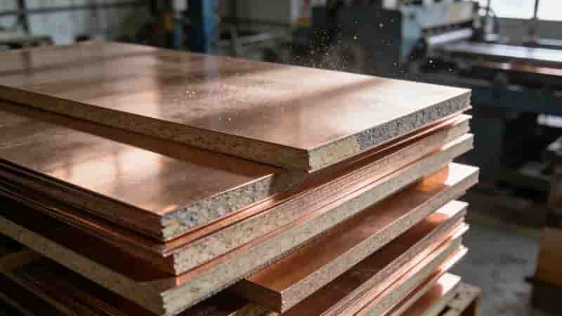
Common cut sizes include 690×620mm, 620×520mm, and 620×347mm. Thin materials use smaller panels to avoid warping; thick materials use larger formats for efficiency.

Automated PCB Cutting Line Edge Sanding Deburring

Automated lines cut and deburr edges to ensure safe handling, accurate alignment, and smooth downstream processing.

Pinning Before Drilling

Before drilling, panels are stacked with backing board to protect machinery and prevent bending. Pinning fixes layers to avoid shifting and misalignment.

PCB Pinning Process Stack Panel Fixing Alignment

Proper pinning ensures high precision for vias, through holes, and mechanical holes in the following steps.

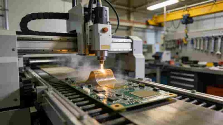
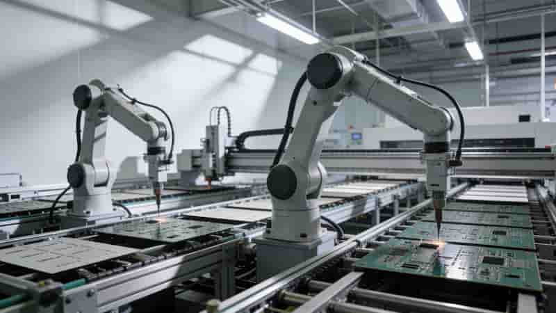
Precision PCB Drilling

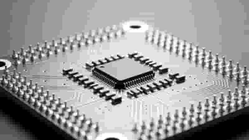
Drilling creates electrical vias, through holes, and mounting holes using high-speed CNC machines. MI parameters control exact position and tool selection.

CNC PCB Drilling Machine Drill Bits 0.2mm Precision

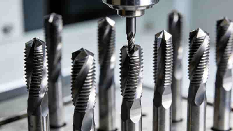
Drill bits range from 0.2mm to 3.0mm in 0.05mm steps. Laser detection checks bit condition before each operation. Bits are maintained at fixed hole counts to keep wall quality and accuracy.

Aluminum foil on top provides heat dissipation and stable drilling. After drilling, panels proceed to copper plating.

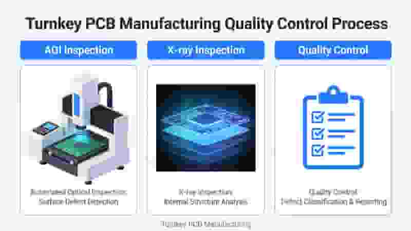
Process Quality Comparison

ProcessPurposeQuality Benefit
MIStandardize production rulesConsistent & stable quality
CuttingPrepare correct panel sizeNo warpage, accurate fitting
PinningFix layer alignmentHigh hole position accuracy
DrillingForm vias & holesReliable conductivity & assembly

Conclusion

MI, cutting, and drilling are the foundational steps of PCB manufacturing. Strict process control ensures dimensional accuracy, high yield, and reliable performance for industrial and commercial applications.

Professional engineering and automated equipment deliver consistent quality that global buyers and engineers trust.

Get Your Custom PCB Solution

Request free DFM check, precise drilling, fast lead time, and reliable PCB manufacturing for your export projects.

Get Free Quote

Rapid Prototype PCB South Africa Quick Turn

PCB Manufacturer in South Africa | Local PCB Manufacturing & Export

Posted on
0 Comments
We are a professional PCB manufacturer in South Africa delivering reliable local PCB manufacturing, prototype, assembly and custom PCB services with high quality and fast delivery. Local PCB Manufacturing in South Africa As a trusted local PCB manufacturer, we provide complete PCB manufacturing in South Africa with cost-effective solutions for industrial, automotive, telecom and medical…
Engineering Teams Using Prototype PCB Assembly

Prototype PCB Assembly Service – Fast, Reliable & Turnkey Solutions

Posted on
0 Comments
Fast prototype PCB assembly with no minimum order quantity, flexible turnkey options and professional engineering support to help you validate designs quickly and reduce time-to-market. Turn your PCB design into fully assembled prototype boards in days, not weeks. We provide dedicated prototype PCB assembly services, combining PCB fabrication, component sourcing, SMT/THT assembly and testing into…
Filled vs Capped Vias PCB Reliability Comparison

Filled and Capped Vias: Boost PCB Reliability for Industrial & Export Applications

Posted on
0 Comments
Filled and capped vias are advanced PCB design techniques that measurably enhance connection reliability. Learn when and why to leverage precision via filling and durable capping to prevent moisture ingress, fractures, and short circuits. Introduction As PCBs become more complex with higher component densities and more demanding performance requirements, the reliability of plated through holes,…
HDI PCB Microvia Types: Blind, Buried, Stacked Vias

HDI PCB Layout and Basic HDI Design Guidelines

Posted on
0 Comments
HDI PCB is an advanced printed circuit board technology for high‑component‑density electronics. This guide covers core HDI PCB layout principles, via design, trace rules, stackup, and IPC standards for engineers and buyers. What Is HDI PCB Layout? High Density Interconnects (HDI PCB) layout refers to advanced PCB design techniques used when trace widths drop below…
Double-Sided Flex PCB Structure Diagram | Flexible Circuit Layer Structure

Double-Sided Flex PCB Manufacturing Services | 2-Layer Flexible PCB Solutions

Posted on
0 Comments
Double-sided flex PCB (also known as 2-layer flexible PCB) is a flexible circuit with two copper conductive layers on polyimide film, connected by plated through holes. We provide full-process manufacturing, customized stackup, strict quality control and fast delivery for global industrial, medical, automotive and high-tech electronics applications from prototype to mass production. What Is a…
Turnkey PCB Manufacturing Quality Control AOI X-ray Inspection

Turnkey PCB Manufacturing and Assembly: Full One-Stop Solution Advantages

Posted on
0 Comments
Turnkey PCB manufacturing and assembly provides a fully integrated end-to-end service covering design for manufacturing (DFM), bare board fabrication, electronic component sourcing, SMT assembly, THT assembly, functional testing, quality inspection and global shipping. This unified model reduces lead times, lowers total costs, improves quality consistency and simplifies project management for international electronics buyers, engineers and…

FAQs About PCB MI, Material Cutting & Drilling Process

A: MI is Manufacturing Instruction, a key engineering document that converts design files into standardized production steps to ensure consistent processing.

A: Raw sheets are 49″×82″ and 49″×41″. Common cut panel sizes include 690×620mm, 620×520mm and 620×347mm.

A: Pinning fixes stacked panels to prevent layer shifting, ensuring high positioning accuracy for holes and vias.

A: Drill bits cover 0.2mm to 3.0mm with 0.05mm increments, and tool status is checked by laser before use.

A: It helps dissipate heat and keep the drilling process stable for better hole wall quality.

A: Thin materials use smaller panels to avoid warpage, while thick materials adopt larger panels for higher production efficiency.

A: It unifies production rules, supports panelization to cut costs, and maintains stable quality across all batches.

A: Drilling creates vias, through holes and mounting holes for electrical connection and component assembly.

Similar Posts