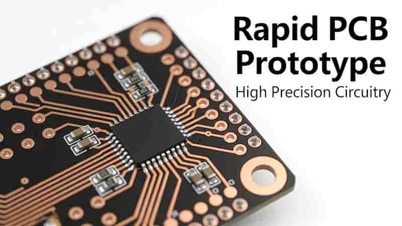
Rapid PCB prototyping delivers fast-turn fabrication from 8 hours for double-sided boards to 24–72 hours for multilayer prototypes. We provide high-quality, IPC Class 2, RoHS & UL certified services to accelerate your product development.
Why Choose Our Rapid PCB Prototyping
In the fast-paced electronics industry, speed and quality are critical. We specialize in professional rapid PCB prototyping and fast‑turn fabrication to help engineers, R&D teams, and enterprises launch products faster.
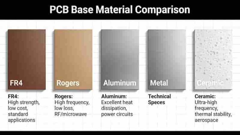
- Full PCB types: single‑sided, double‑sided, multilayer, rigid, flexible & rigid‑flex
- Ultra‑fast lead times: 8 hours for double‑sided prototypes; 24–72 hours for small batches
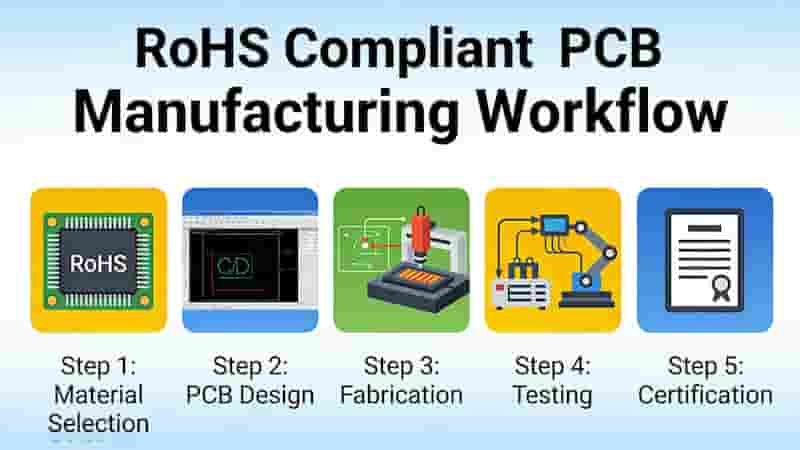
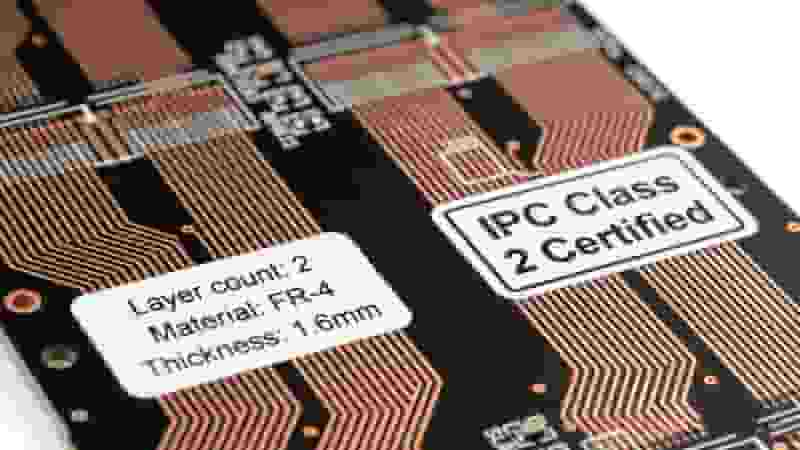
- High quality: IPC Class 2, RoHS and UL certified
- Low MOQ: 5–100 pieces for iterative design testing
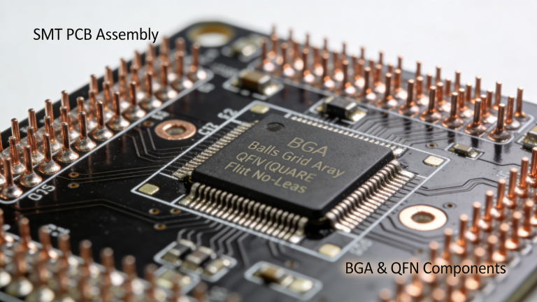
- One‑stop service: PCB manufacturing + SMT/THT assembly + component sourcing

What Is Rapid PCB Prototyping
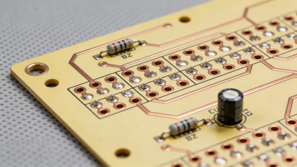
Rapid PCB prototyping produces small‑batch printed circuit boards to test and validate designs before mass production. It helps engineers detect flaws early and ensure final products meet performance and reliability standards.
Speed
Prototypes as fast as 8 hours for double‑sided PCBs, 24–72 hours for multilayer boards.
Flexibility
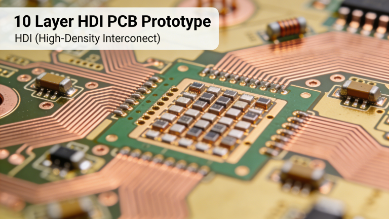
Supports complex designs including multilayer PCBs with blind or buried vias.
Cost Efficiency
Reduce expensive mass‑production revisions by validating designs early.
Benefits of Fast-Turn PCB Prototyping
Our rapid PCB prototyping service helps you stay competitive and build better products with less risk.
- Speed Up Time-to-Market: Launch products faster with 8-hour quick‑turn prototypes
- Ensure Flawless Designs: Test and optimize early to avoid production failures
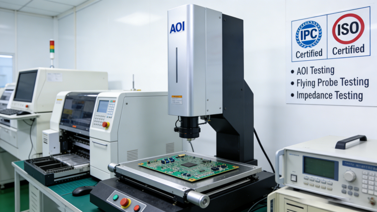
- Maintain High-Quality Standards: IPC Class 2, RoHS & UL compliant for industrial use
- Reduce Total Costs: Low MOQ and fewer revisions lower overall development cost
- Support Complex Customization: Multilayer, flexible, rigid‑flex and high‑precision designs

Why We Stand Out
- Advanced Equipment: Automated production lines ensure precision and fast delivery
- Professional Engineering: Free Gerber review & DFM optimization suggestions
- Global Service: Reliable delivery to USA, Canada, UK, Europe, Australia & worldwide
- 24/7 Support: Fast response to all your inquiries and project needs
Rapid PCB Prototyping Turnaround Time
| Layers | ≤0.1㎡ | Normal | 0.1‑1㎡ | Normal | 1‑2㎡ | Normal |
|---|---|---|---|---|---|---|
| Single-layer | 24H | 3 Days | 24H | 4 Days | 3 Days | 5 Days |
| Double-layer | 24H | 4 Days | 2 Days | 5 Days | 3 Days | 7 Days |
| 4 Layer | 2 Days | 6 Days | 3 Days | 7 Days | 4 Days | 8 Days |
| 6 Layer | 3 Days | 7 Days | 4 Days | 8 Days | 5 Days | 10 Days |
| 8 Layer | 3 Days | 9 Days | 4 Days | 10 Days | 6 Days | 11 Days |
How to Get Started
- Prepare Gerber files and specify layer count, quantity and delivery requirements
- Email us for a free, fast quotation based on your needs
- Choose expedited rapid PCB prototyping service
- Full quality inspection following international standards
- Fast global delivery to your door
Summary
Rapid PCB prototyping is essential for modern electronics development. We combine ultra‑fast lead times, strict quality control, low MOQ, and professional support to help you innovate faster and reduce risks.
Request Your Rapid PCB Prototyping Quote
Get DFM‑optimized boards in as fast as 24 hours. 100% quality guaranteed. Send your Gerber files now for an instant quote.
Rapid PCB Prototyping Services: A Comprehensive Introduction
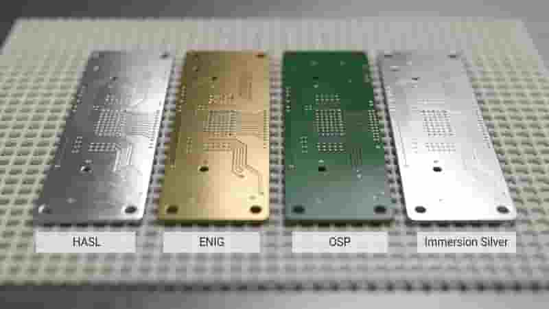
Choosing the Right PCB Surface Finish for Your Project in 2025
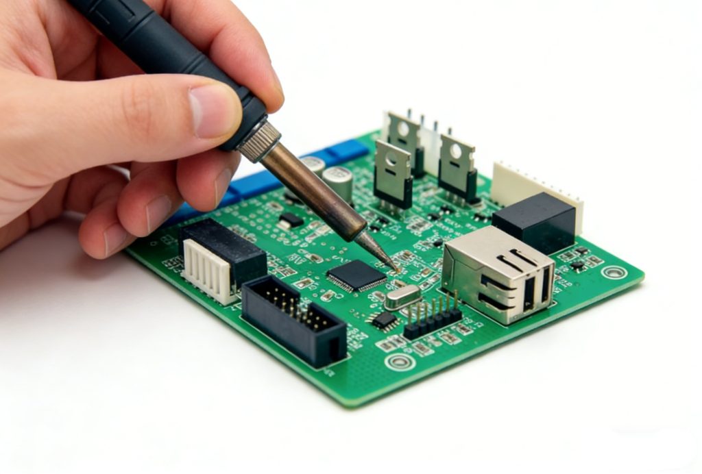
What is a Pad in PCB Design?
Accelerate Your Innovation with Rapid PCB Prototyping
Single Layer PCB Manufacturing | Affordable Single Sided PCBs