As a trusted PCB manufacturer in China, we specialize in high-quality double-layer PCB solutions. With over 15 years of experience, we deliver boards tailored to your needs, from prototypes to mass production.
Why Choose Us for Double Sided PCBs?
Advanced Technology
Supports complex multilayer routing and compact designs.
No MOQ
Ideal for startups and large projects.
Quick-Turn Prototyping
24-hour delivery for double sided PCB prototypes.
Free DFM Analysis
Optimize designs to save costs and avoid production issues.

What is a Double Sided PCB?
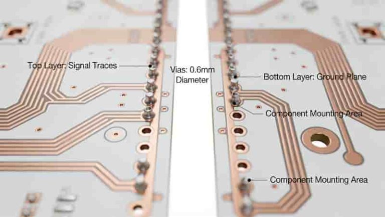
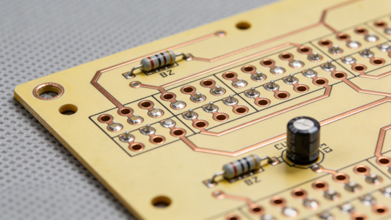
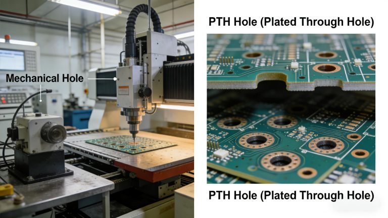
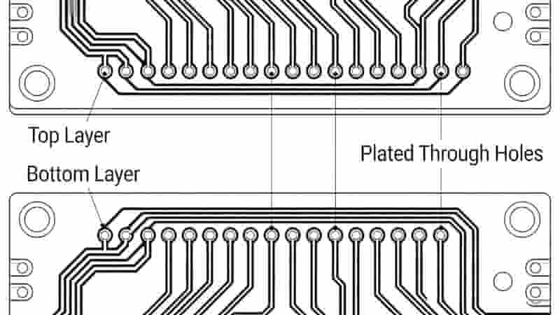
A double-sided PCB, also known as a double-layer PCB or 2-layer PCB, features conductive copper layers on both sides of a substrate, typically FR4. This design enables components and circuits on both top and bottom layers, connected via plated-through holes (vias) for enhanced functionality.
Key Features
- Higher Component Density: Supports compact designs for mobile phones and IoT gadgets.
- Flexible Routing: Vias enable complex connections not possible on single-sided PCBs.
- Wide Applications: Used in LED lighting, automotive dashboards, and RF systems.
Types of Double Sided PCB
We manufacture various double sided PCB types to suit diverse applications:
- Rigid PCB: FR4 substrate for consumer electronics and LED lighting.
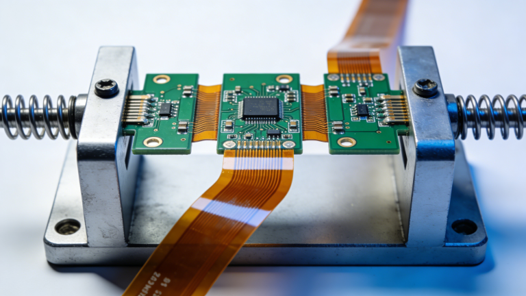
- Flexible PCB: Polyimide material for wearables and dynamic devices.
- Metal Core PCB: Aluminum core for superior heat dissipation in high-power LEDs.
- High Tg PCB: Excellent thermal stability for industrial controls.
- High Frequency PCB: Rogers material for RF and microwave circuits.
- Heavy Copper PCB: Thick copper for power electronics and industrial drives.
- Impedance Control PCB: Ensures signal integrity for high-speed applications.
Double Sided PCB Stack-Up
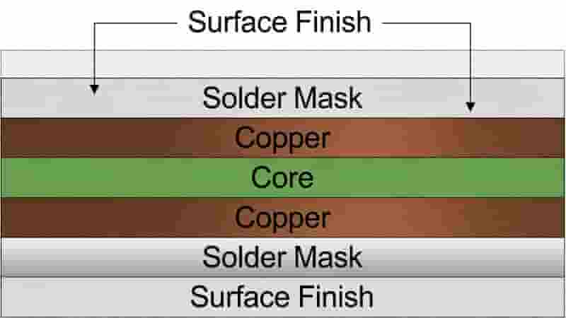
Understanding the stack-up is critical for reliable double sided PCB design. We ensure precision in every layer:
Core Layers
- Top Conductive Layer: Copper for conductivity; finished with gold/silver as needed.
- Dielectric/Base Layer: FR4, Polyimide, or PTFE for insulation.
- Bottom Conductive Layer: Mirrors the top layer for dual-sided circuits.
Protective Layers
- Surface Finish: OSP, Immersion Gold, Tin to prevent oxidation.
- Solder Mask: Prevents solder bridges and environmental damage.
- Silkscreen: Labels components for easy assembly.
Benefits of Double Sided PCBs
- Increased Component Density: Double the space for compact designs.
- Flexible Routing: Vias and dual layers reduce congestion.
- Better Signal Integrity: Ground planes minimize noise.
- Space-Saving: Up to 50% smaller than single-sided equivalents.
- Cost-Effective: Affordable alternative to multilayer PCBs.
Double Sided PCB Prototyping
We provide rapid double sided PCB prototype fabrication for LED systems, wearables, and RF circuits.
- Materials: FR4, metal-core, flexible polyimide
- Finishes: Immersion Gold, OSP, Lead-Free Tin
- Speed: 24-hour quick-turn available
Double-Sided PCB Fabrication Capabilities
We are a trusted double-sided PCB manufacturer in China, with expertise in quick-turn prototyping and mass production.
| Parameter | Details |
|---|---|
| Materials | FR4, Copper Core, Aluminum, Rogers |
| PCB Size | Up to 680mm x 1200mm |
| Thickness | 0.2mm – 6.0mm (customizable) |
| Surface Finishes | OSP, Immersion Gold/Silver/Tin, Plated Gold |
| Solder Mask | Green, Red, White, Black, Blue, Yellow |
Double Sided PCB Assembly Process
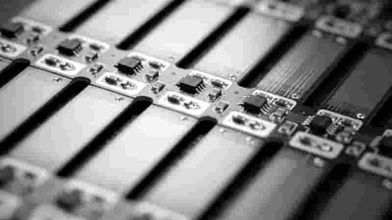
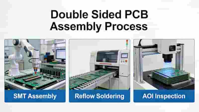
Our assembly uses advanced SMT and THT for precision and reliability:
- Solder Paste Printing on both sides
- Pick and Place components
- Reflow Soldering
- Automated and visual inspection
Double Sided PCB Manufacturing Process
- DFM Check – Verify design for manufacturability
- Drilling & PTH – Create plated through holes
- Plating & Etching – Form precise copper traces
- Surface Finish & Testing – Ensure quality and reliability
Applications of Double Sided PCBs
- Consumer Electronics: Phones, LED lighting
- Power Applications: Inverters, UPS
- Industrial Systems: HVAC, controls
- Automotive: Dashboards, sensors
Frequently Asked Questions
Single vs Double Sided PCB?
Double-sided PCBs have copper on both sides, higher density, better signal integrity.
Prototype lead time?
24-hour quick-turn available for double sided PCB prototypes.
Surface finishes?
OSP, Immersion Gold, Lead-Free Tin, and more.
MOQ?
No MOQ – from 1 piece to mass production.
Get Your Free Double Sided PCB Quote
Upload your Gerber files for a free DFM analysis and instant quote for double sided PCB manufacturing.