This professional PCB glossary provides clear, industry-standard definitions for over 150 key terms used in PCB design, manufacturing, assembly, and quality control. Ideal for engineers, procurement teams, and global buyers, this resource helps streamline communication, avoid misunderstandings, and ensure accurate project execution. We continuously update this list to cover the latest technologies and standards in the PCB industry.
Basic PCB Terms
PCB (Printed Circuit Board): A rigid or flexible substrate that supports and connects electronic components via conductive copper pathways, serving as the core platform for electronic assemblies.
PCBA (Printed Circuit Board Assembly): The process of soldering electronic components onto a bare PCB to create a functional assembly.
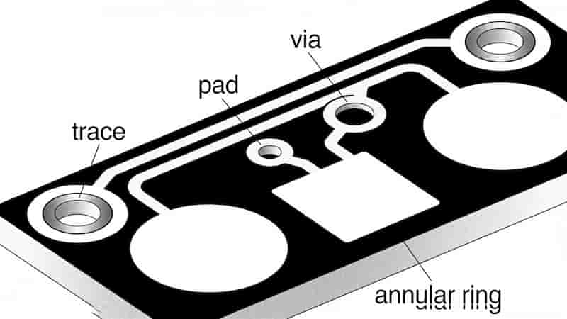
Trace: Conductive copper path on a PCB that transmits electrical signals and power between components.
Pad: Metallic contact area where component leads are soldered to the PCB surface for electrical connection.
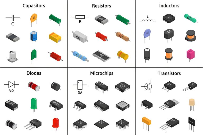
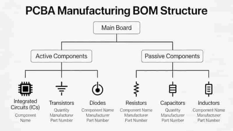
Component: Basic electronic parts such as resistors, capacitors, and integrated circuits mounted on a PCB.
Silkscreen: A printed layer on PCB that marks component positions, names, and polarity for assembly and maintenance.
PCB Materials & Lamination
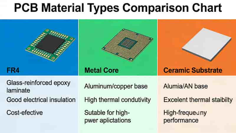
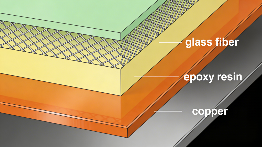
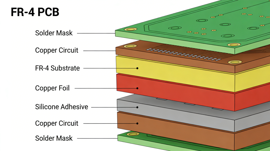
FR-4: The most widely used flame-resistant rigid PCB substrate material, made of glass-reinforced epoxy laminate.
Prepreg (PP): Resin-impregnated fiberglass used to bond layers in multilayer PCB manufacturing.
Copper Clad Laminate (CCL): Base material for PCB fabrication, consisting of a dielectric core bonded with copper foil.
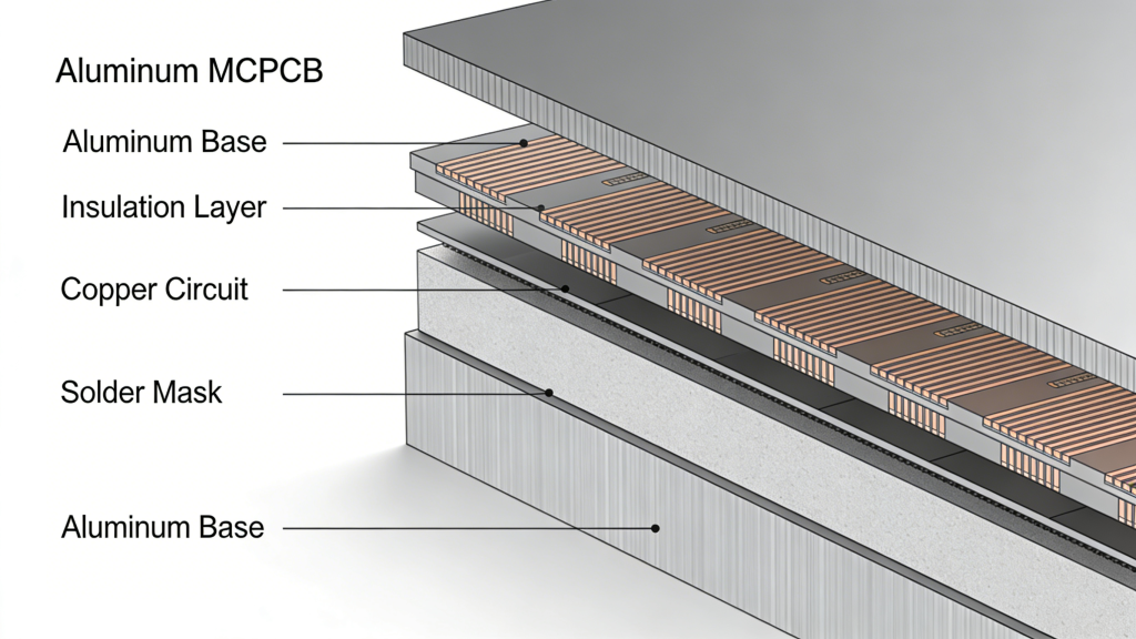
Metal Core PCB: PCB with a metal base (aluminum/copper) for excellent thermal dissipation in high-power applications.
Substrate: The base insulating material of a PCB, such as FR-4, aluminum, ceramic, or flexible polyimide.
PCB Structure & Layers
Single-Sided PCB: PCB with conductive traces and components on only one side.
Double-Sided PCB: PCB with conductive circuits on both top and bottom sides.
Multilayer PCB: PCB with three or more conductive layers stacked and bonded together for high-density designs.
HDI PCB (High-Density Interconnector): Advanced PCB technology using micro vias for ultra-high component density.
Ground Plane: A full conductive layer in a PCB used for grounding and signal integrity.
Via & Hole Technology
Via: Plated through-hole that connects different layers in a multilayer PCB.
Through-hole Via: Via that penetrates all layers of a PCB.
Blind Via: Via that connects an outer layer to one or more inner layers but does not pass through the entire board.
Buried Via: Via that connects only inner layers of a PCB and is not visible from the outside.
Annular Ring: Copper ring surrounding a drilled via, critical for reliable electrical connection in PCB design.
Aspect Ratio: Ratio of PCB thickness to minimum via diameter, affecting plating quality.
PCB Assembly (SMT/THT)
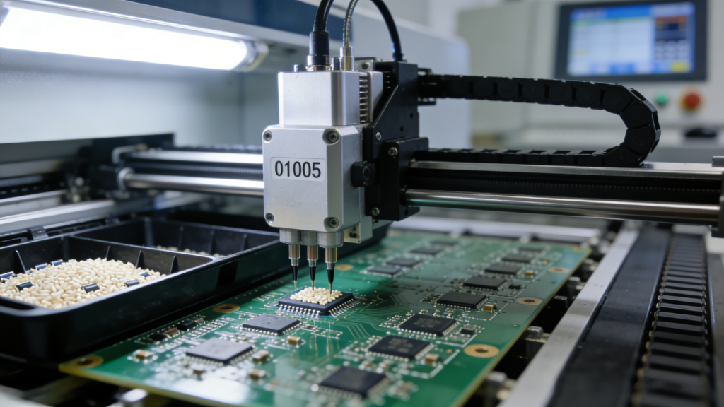
SMT (Surface Mount Technology): Assembly method that solders components directly onto PCB surface for high density.
SMD (Surface Mount Device): Components designed for surface mounting on PCB.
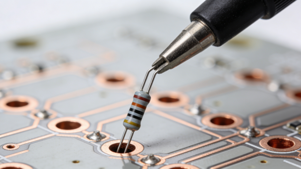
THT (Through-Hole Technology): Assembly method that inserts component leads through PCB holes for soldering.
BGA (Ball Grid Array): High-density IC package soldered to PCB using solder balls.
Reflow Soldering: Process of melting solder paste to attach SMD components to PCB pads.
Pick and Place: Automated process that places SMD components accurately onto PCB.
Surface Finish & Coating
Solder Mask: Protective insulating layer applied to PCB copper traces to prevent short circuits and oxidation.
HASL (Hot Air Solder Level): Common PCB surface finish using molten solder.
ENIG (Electroless Nickel Immersion Gold): Premium PCB surface finish for fine-pitch components and wire bonding.
OSP (Organic Surface Protectant): Environmentally friendly organic coating for PCB copper protection.
Gold Fingers: Gold-plated edge connectors on PCB for reliable connection between boards.
Quality & Inspection Standards
IPC: Global association that sets international standards for PCB design and manufacturing.
AOI (Automated Optical Inspection): Machine vision system to inspect PCB assembly quality.
Electrical Test: Test to verify PCB continuity and isolation (open/short circuits).
AQL (Acceptance Quality Limit): Quality standard defining acceptable defect rate in PCB production.
RoHS: European directive restricting hazardous substances in PCB and electronic products.
Design & Manufacturing Files
Gerber File: Standard PCB design file used for manufacturing and fabrication.
NC Drill File: File containing PCB hole coordinates and sizes for CNC drilling.
CAM File: Computer-aided manufacturing file for PCB production control.
DFM (Design for Manufacturing): PCB design optimization for reliable and cost-effective production.
Common Industry Abbreviations
| Term | Abbreviation | Full Name |
|---|---|---|
| Printed Circuit Board | PCB | Printed Circuit Board |
| Surface Mount Technology | SMT | Surface Mount Technology |
| Automated Optical Inspection | AOI | Automated Optical Inspection |
| Design for Manufacturing | DFM | Design for Manufacturing |
Key Technology Comparison
| Item | SMT | THT |
|---|---|---|
| Component Type | SMD | Through-hole components |
| PCB Density | High | Low |
| Application | Consumer electronics, high-tech devices | Power equipment, industrial controls |
Summary
This PCB terminology glossary covers core concepts in PCB design, materials, manufacturing, assembly, and quality control. Understanding these terms helps engineers, buyers, and project managers communicate clearly, reduce errors, and ensure smooth PCB production. We keep expanding this glossary to include emerging technologies and industry updates.
Whether you are sourcing PCB products, designing circuits, or managing manufacturing projects, this glossary serves as a reliable reference to support your work.
Ready to Start Your PCB Projects?
We provide professional PCB manufacturing & assembly services with fast delivery, strict quality control, and full IPC standards compliance. Get your free quote now!
What is FR-4 Material in PCB Fabrication? The Complete Engineering Guide
What is FR-4 Material in PCB Fabrication? Complete Engineering Guide
What is a Surface Mount Device or SMD Component Package?
Turnkey PCB Assembly Services | Full & Partial Solutions
Through-hole PCB Assembly Service | IPC Certified THT PCBA Solutions