What is SMD? Surface Mount Device Guide
Whether you work in the electronic assembly industry or not, you’ve likely heard terms like SMD or SMT. These are quite common—if you have any connection to technology, you’ll often see and hear these words in your day-to-day.
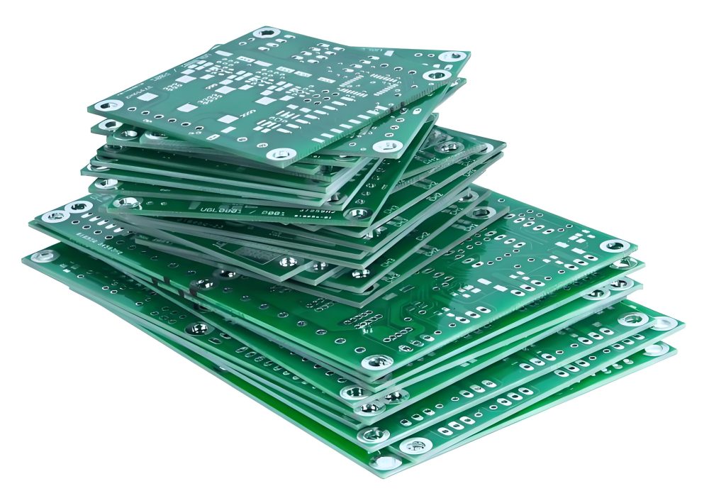
Nearly all mass-produced electronic products use surface mount technology (SMT), but not every component can be made into a surface mount device (SMD). In SMT processes, surface mount components are the most widely used type, though through-hole technology (THT) components are still in use too.
These industry-specific professional terms can sometimes leave people confused. It’s common to hear questions like, “What is SMT?” or “What is SMD?” Understanding these terms is essential—only by grasping their definitions can you gain a deeper understanding of the electronic assembly industry.
Understanding SMD and SMT
SMD is the abbreviation for Surface Mount Devices. It refers to the components used in Surface Mount Technology (SMT)—so SMD is also known as SMC, short for Surface Mount Component.
SMD comes in a variety of package forms, and most of these forms follow standardized production. This standardization has not only made automated PCB assembly possible but also simplified the process.
The table below lists key terms related to surface mounting:
| SMT Term | Expanded Form |
|---|---|
| SMD | Surface-mount devices (active, passive, and electromechanical components) |
| SMT | Surface-mount technology (assembling and mounting technology) |
| SMA | Surface-mount assembly (module assembled using SMT) |
| SMC | Surface-mount components (components designed for SMT) |
| SMP | Surface-mount packages (case forms for SMDs) |
| SME | Surface-mount equipment (machines used for SMT assembly) |
The Difference Between SMD and SMT
What is SMT?
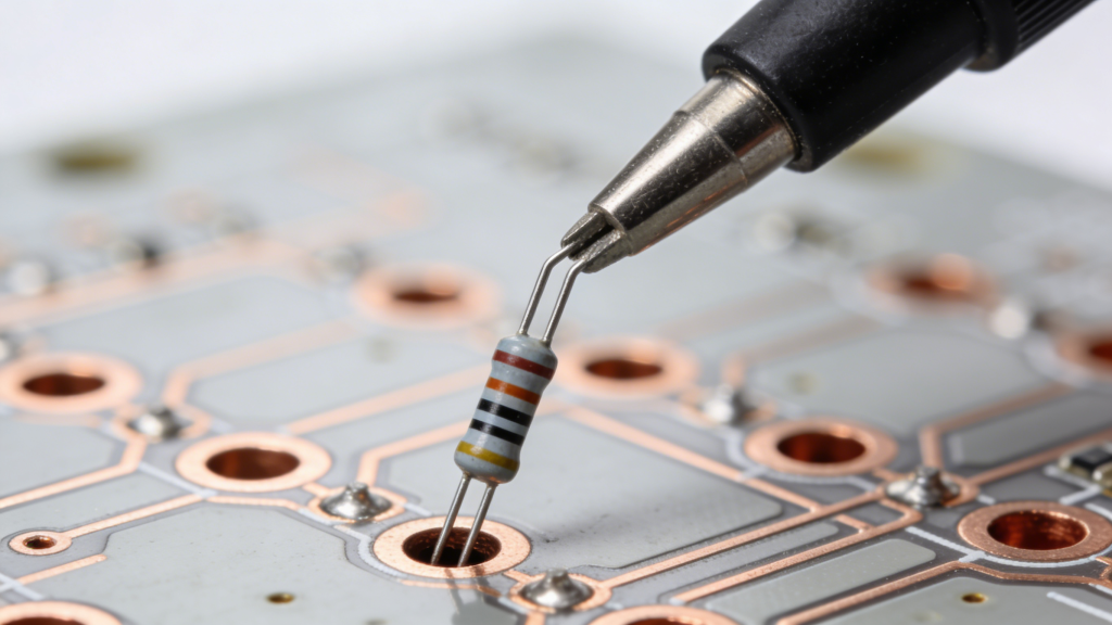
SMT—short for Surface Mount Technology—is a next-generation PCB assembly method. The other main type of PCB assembly technology is Through-Hole PCB assembly. Importantly, SMT is a technology, not a component.
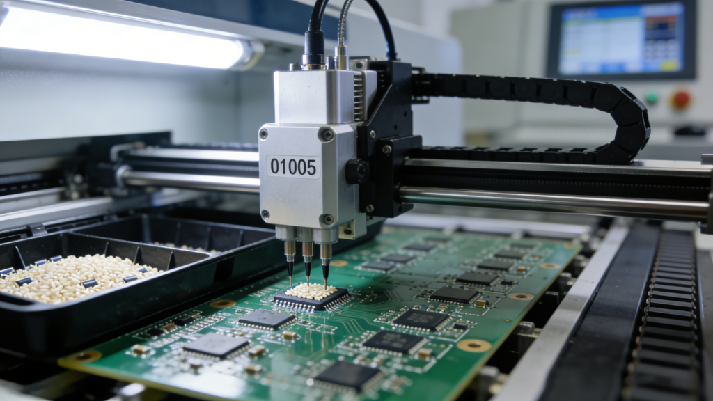
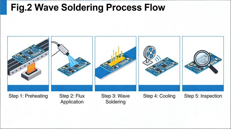
As a circuit board assembly technology, SMT is widely used in the modern electronic assembly industry. The full SMT process can be divided into five stages, including single-sided and double-sided assembly. The equipment required for SMT production includes solder paste printers, placement machines, reflow ovens, optical inspection machines, dispensers, and more.
Surface mount technology has strict requirements for production workshop conditions. Typically, it requires a dust-free workshop with constant temperature and low humidity. Additionally, workshop staff must wear dust-free clothing, anti-static shoes, gloves, and other protective gear.
Now that we’ve covered SMT in detail, let’s turn to understanding SMD.
Characteristics of SMD
The key feature of SMDs lies in their distinct shape and structure, which set them apart from traditional through-hole components. Their specific traits include:
- Compact and lightweight: SMDs have small sizes, light weights, short leads (or even no leads at all), and high overall reliability.
- Strong resistance performance: They can withstand shock, vibration, and external interference effectively.
- Easy automation integration: SMDs support both semi-automatic and fully automatic assembly. Most SMDs use tape-and-reel, tube, or tray packaging—this design directly helps boost assembly efficiency.
- High-density assembly capability: Thanks to their small size, SMDs enable dense component placement on circuit boards. Their solder joint failure rate is extremely low, at less than 10 parts per million (ppm).
- Superior high-frequency performance: Using SMD mounting allows electronic circuits to operate at frequencies up to 3000MHz (compared to just 500MHz for traditional through-hole insertion).
- Reduced parasitic parameters: This advantage helps improve the high-frequency characteristics and operating speed of electronic equipment.
- Precise dimensional consistency: SMD products feature high dimensional accuracy, ensuring uniform performance across batches.
SMD-Adopted Technologies
(1) Laminated Process Technology
In the past, three main process methods dominated:
- Mechanical perforation process (dry method)
- Overlap printing process (wet method)
- Internal connection process (wet method)
However, these three technologies had inherent drawbacks—they struggled to efficiently produce smaller, more precise chip components.
Today, the mechanical perforation connection process has been significantly upgraded, incorporating laser perforation, close printing, and automatic microporous grouting technology. This advancement has reduced the aperture to 50μm (with a position accuracy of ±20μm) and narrowed printing line widths and spacing to 50μm (with a position accuracy of ±10μm). Leveraging this advanced process, we can manufacture smaller, more refined chip components and low-temperature co-fired ceramic (LTCC) passive integrated components.
(2) Ultra-Thin Dielectric Layer and Nano-Powder Technology
Currently, the capacitance of chip multilayer ceramic capacitors (MLCCs) has been increased to 100μF and put into practical application. This breakthrough is largely supported by ultra-thin dielectric layer and nano-powder technology— the thin, uniform dielectric layer is a direct indicator of the current development level of ultra-thin dielectric technology.
To make ceramic dielectric layers as thin as 1μm, the ceramic powder must have a nano-scale particle size. Additionally, cost considerations require replacing Ag/Pd (silver/palladium) electrodes with metal electrodes, while increasing the number of capacitor layers to hundreds. As a result, the development of anti-reduction nano-ceramic powder has become a critical issue—and significant progress has been made in this field both domestically and internationally.
(3) Thin-Film Technology
In previous years, thin-film technology was mainly used to produce thin-film circuits (typically for microwave integration). This approach had two major limitations: high production costs and small production scales.
In recent years, thin-film manufacturing technology has advanced dramatically. Beyond traditional physical methods, chemical methods have emerged as highly effective alternatives—pushing thin-film technology into a low-cost, large-scale production model. Chip components made using this process offer three key advantages: small size, excellent high-frequency characteristics, and easy integration into larger systems.
(4) Semiconductor Microelectronics Technology
In the last two decades of the 20th century, semiconductor microelectronics technology achieved remarkable progress—advancing from micron-level to sub-micron, then to deep sub-micron precision. It also delivered high productivity, low costs, and strong reliability. Currently, China’s production level in this field has reached 0.18μm.
In contrast, passive component manufacturing technology lagged behind for years. However, in recent years, passive component producers have started learning from and adopting semiconductor microelectronics technology—and this strategic move has yielded immediate, positive results.
The Development Trend of SMD
Driven by market demand, SMDs are constantly improving in performance while their package sizes continue to shrink. In particular, significant progress has been made in expanding parameter ranges, enhancing current/power handling capabilities, enabling lead-free production, and boosting overall reliability.
(1) Miniaturization & Thin Profiling
In the past, many believed the 1005 package (1.0×0.5mm) was the smallest possible size for chip components—since such tiny packages would create major challenges for mounting processes. However, advancements in surface mount technology have made even smaller packages (0.4×0.2×0.2mm) the current mainstream. Importantly, the reduction in chip component package sizes shows no sign of stopping; they will keep developing toward further miniaturization. It remains to be seen just how small SMD packages can become in the future.
(2) Arrayization & Componentization
To simplify application and reduce the space occupied on PCBs (printed circuit boards), various chip components are now being designed in array formats.
(3) Integration & LTCC
Passive integration is a key current development direction, and low-temperature co-firing ceramic (LTCC) technology is the most suitable solution for passive integration. Well-known international companies—such as National Semiconductor, Motorola, and Murata—have already produced large volumes of LTCC products, including radio frequency (RF) modules and Bluetooth modules. These modules are widely used, and their technical complexity is constantly increasing.
LTCC technology traditionally faced three major technical challenges: simulation design, specialized materials, and high-precision process equipment. However, companies both at home and abroad have now overcome these difficulties.
(4) High-Frequency (Radio Frequency/Microwave) Capabilities
Modern electronics are trending strongly toward higher frequencies, and most of these devices are portable. Traditional microwave components can no longer meet these evolving needs—this demand gap is driving the rapid and vigorous development of chip-based high-frequency (RF/microwave) components.
Specifications of SMD Components
As SMT (Surface Mount Technology) advances, the industry has established a set of easy-to-implement standards for SMD components. All component suppliers now manufacture products in strict compliance with these standards.
Below are the standard dimensions for common SMD components:
The Size of SMD Components
Common Passive SMD Package Details
| SMD Package Type | Dimensions (mm) | Dimensions (inches) |
|---|---|---|
| 2920 | 7.4 x 5.1 | 0.29 x 0.20 |
| 2725 | 6.9 x 6.3 | 0.27 x 0.25 |
| 2512 | 6.3 x 3.2 | 0.25 x 0.125 |
| 2010 | 5.0 x 2.5 | 0.20 x 0.10 |
| 1825 | 4.5 x 6.4 | 0.18 x 0.25 |
| 1812 | 4.6 x 3.0 | 0.18 x 0.125 |
| 1806 | 4.5 x 1.6 | 0.18 x 0.06 |
| 1210 | 3.2 x 2.5 | 0.125 x 0.10 |
| 1206 | 3.0 x 1.5 | 0.12 x 0.06 |
| 1008 | 2.5 x 2.0 | 0.10 x 0.08 |
| 0805 | 2.0 x 1.3 | 0.08 x 0.05 |
| 0603 | 1.5 x 0.8 | 0.06 x 0.03 |
| 0402 | 1.0 x 0.5 | 0.04 x 0.02 |
| 0201 | 0.6 x 0.3 | 0.02 x 0.01 |
| 01005 | 0.4 x 0.2 | 0.016 x 0.008 |
SMD component sizes are represented by 4 digits:
- The first two digits indicate the length
- The last two digits indicate the width
- The unit for the 4-digit code is 0.01 inches (or 10 mils).
For example, the three most widely used SMD sizes are:
- 0603: Represents 0.06″ x 0.03″ (or 60 x 30 mils, or 1.6 x 0.8 mm)
- 0805: Represents 0.08″ x 0.05″ (or 80 x 50 mils, or 2.0 x 1.25 mm)
- 1206: Represents 0.12″ x 0.06″ (or 120 x 60 mils, or 3.2 x 1.6 mm)
Types of SMD
SMDs come in a wide variety of types, each with a unique package design—collectively forming a comprehensive library of surface mount components.

1. Broad Classification of SMD Components
(1) Connecting Members (Interconnects)
These components enable mechanical and electrical connection or disconnection, typically consisting of plugs and sockets. While they may connect to cables, brackets, or chassis, their actual attachment to circuit boards relies on surface-mounted contacts.
(2) Active vs. Passive Electronic Components
Active Electronic Components: These include analog or digital circuits that can control voltage and current to generate gain (amplification) or switching actions. They respond to applied signals and may change their fundamental characteristics.
Passive Electronic Components: Unlike active components, these do not alter their own characteristics when an electrical signal is applied. Instead, they provide a simple, consistent response (e.g., storing charge or resisting current).
(3) Shaped Electronic Components (Odd-Form)
These components have irregular geometric dimensions, so they must be mounted manually. Their housing shapes (distinct from their core functions) are non-standard. Examples include transformers, hybrid circuit structures, fans, and mechanical switch blocks.
2. Other SMD Classifications
By different standards, SMDs can also be categorized into chip transistors and integrated circuits (ICs). Integrated circuits further include various package types such as SOP, SOJ, PLCC, LCCC, QFP, BGA, CSP, FC, and MCM.
3. Common SMD Component Types (with PCB Identifiers)
Below is a brief introduction to the most widely used SMD components. Note: The letters in parentheses represent their labels on PCBs (printed circuit boards).
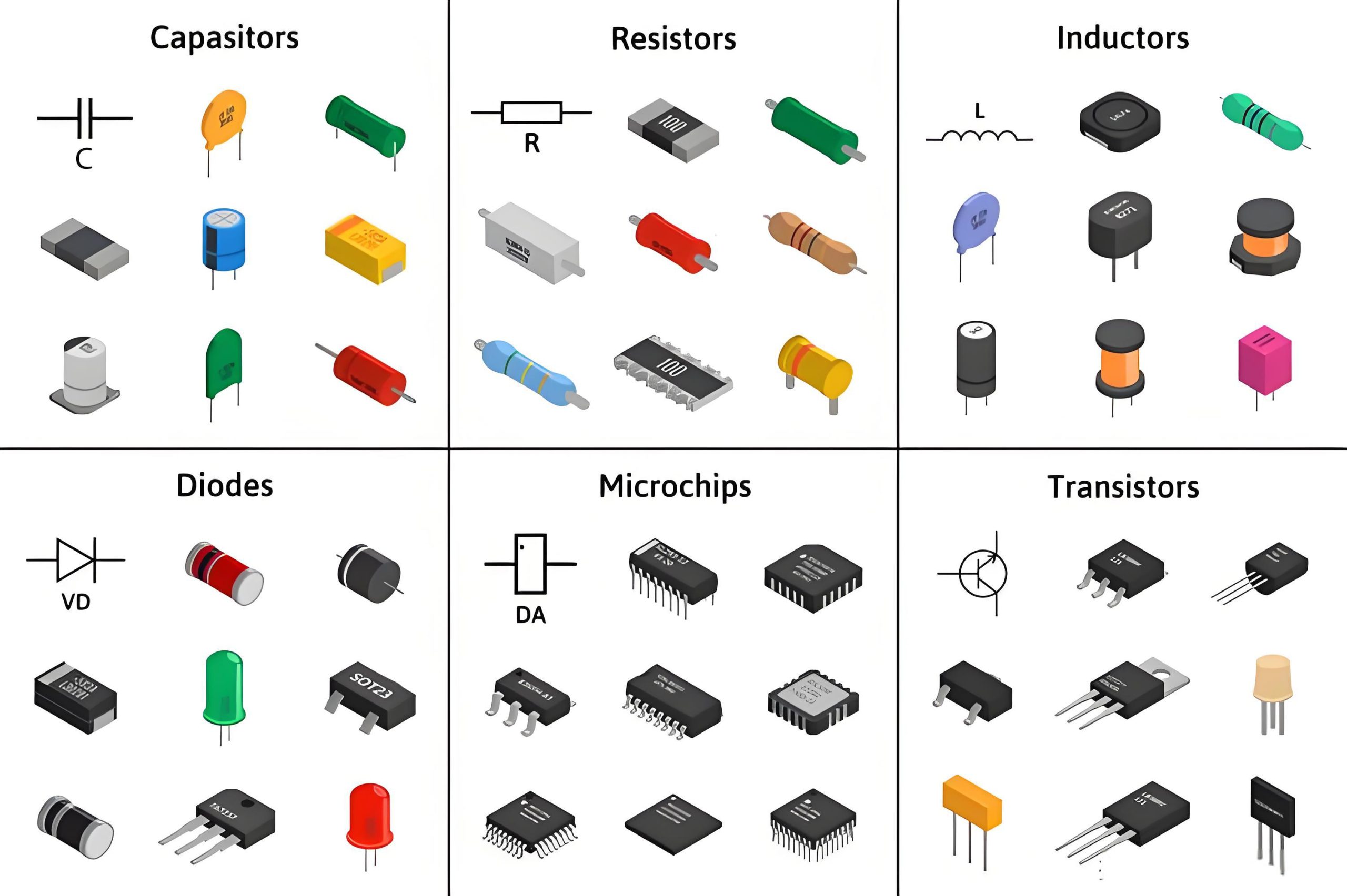
• Chip Resistor (R)
- A 3-digit code on the resistor indicates its resistance value:
- The first two digits are significant figures.
- The third digit represents the number of zeros (i.e., multiples of 10).
- Examples:
- “103” = 10 × 10³ Ω = 10KΩ
- “472” = 47 × 10² Ω = 4700Ω
- The letter “R” denotes a decimal point (e.g., R15 = 0.15Ω).
• Network Resistor (RA/RN)
- Encapsulates multiple resistors with identical parameters, commonly used in digital circuits.
- Its resistance identification method is the same as that of chip resistors.
• Capacitor (C)
- The most widely used type is MLCC (Multi-layer Ceramic Capacitor), classified by material into COG (NPO), X7R, and Y5V—with COG (NPO) offering the highest stability.
- Other common types include tantalum capacitors and aluminum capacitors; note their polarity when installing.
• Diode (D)
- A widely used SMD component. Typically, a colored band on the diode body indicates the direction of its negative terminal.
• LED (LED)
- Divided into standard LEDs and high-brightness LEDs, available in colors like white, red, yellow, and blue.
- Determine LED polarity based on the specific product’s manufacturing guidelines.
• Triode (Q)
- Common structures include NPN and PNP, covering types like Triode, BJT (Bipolar Junction Transistor), FET (Field-Effect Transistor), and MOSFET.
- The most popular SMD packages are SOT-23 (smaller) and SOT-223 (larger).
• Inductor (L)
- Its inductance value is usually printed directly on the component body.
• Transformer (T)
- Functions to step up or step down AC voltage.
• Crystal Oscillator (X)
- Primarily used to generate oscillation frequencies in various electronic circuits.
• Fuse
- Breaks the circuit automatically when excessive current flows through it (protecting other components).
• Integrated Circuit (IC, U)
The most critical functional component in electronic products, with relatively complex package designs (detailed explanation will follow later).
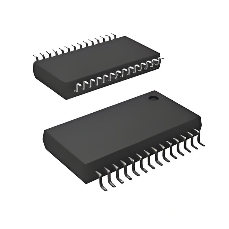
Types of SMD Packages
SMD packages come in diverse designs to suit different component functions and application needs. Below is a detailed breakdown of common SMD package types:
1. BGA (Ball Grid Array)
A surface-mount package featuring an array of spherical solder contacts (bumps) on the back of the printed circuit board (PCB)—these bumps replace traditional pins. The LSI (Large-Scale Integration) chip is mounted on the front of the PCB, then sealed with molding resin or potting compound.
- Key Advantages:
- Supports over 200 pins, ideal for multi-pin LSI components.
- Smaller package size than QFP (Quad Flat Package): For example, a 360-pin BGA (1.5mm pin pitch) is only 31mm², while a 304-pin QFP (0.5mm pitch) is 40mm².
- Eliminates QFP’s common pin deformation issue.
- Background: Developed by Motorola (US), initially used in portable phones. Later adopted for personal computers, with early versions having 225 pins (1.5mm pitch); some manufacturers now develop 500-pin BGAs.
- Challenges: Post-reflow soldering inspection is difficult—no universal visual inspection method exists yet. Many rely on functional testing, as the large solder pitch ensures stable connections.
- Variants: Motorola labels resin-sealed BGAs as “OMPAC” and potting-sealed ones as “GPAC.”
2. BQFP (Bumpered Quad Flat Package)
A type of QFP with small protrusions (buffer pads) at the four package corners. These bumpers prevent pin bending/deformation during transportation.
- Applications: Used by US semiconductor manufacturers for ASICs (e.g., microprocessors).
- Specs: Pin pitch ~0.635mm; pin count ranges from 84 to 196.
3. Butt Welding PGA (Butt Joint Pin Grid Array)
Another term for surface-mount BGA (see “BGA” above).
4. C- (Ceramic)
A labeling prefix indicating a ceramic package. For example, “CDIP” stands for Ceramic DIP (Dual In-line Package). Widely used in industry documentation.
5. Cerdip (Ceramic Dual In-line Package)
A ceramic DIP sealed with glass, used for ECL RAM, DSPs (Digital Signal Processors), and similar circuits. Versions with glass windows are used for UV-erasable EPROMs.
- Specs: Pin pitch 2.54mm; pin count 8–42.
- Regional Naming: In Japan, it is labeled “DIP-G” (G = glass seal).
6. Cerquad
A surface-mount, ceramic-sealed QFP, primarily for DSPs and logic LSIs. Windowed versions are used for EPROMs.
- Key Advantages: Better heat dissipation than plastic QFPs—supports 1.5–2W power under natural air cooling.
- Drawback: 3–5x more expensive than plastic QFPs.
- Specs: Pin pitches include 1.27mm, 0.8mm, 0.65mm, 0.5mm, 0.4mm; pin count 32–368.
7. CLCC (Ceramic Leaded Chip Carrier)
A ceramic chip carrier with T-shaped pins extending from all four sides. Windowed variants are used for UV-erasable EPROMs and EEPROM-based microcontrollers.
- Alternative Names: Also called “QFJ” or “QFJ-G” (see “QFJ”).
8. COB (Chip on Board)
A bare-chip mounting technology where the semiconductor chip is directly attached to a PCB. Electrical connections between the chip and PCB are made via wire bonding, then covered with resin for protection.
- Pros: Simple manufacturing process.
- Cons: Lower packaging density than TAB (Tape Automated Bonding) or flip-chip bonding.
9. DFP (Dual Flat Package)
An outdated term for SOP (Small Out-line Package) (see “SOP”). Once common, it is no longer used in modern documentation.
10. DIC (Dual In-line Ceramic Package)
Another name for ceramic DIP (including glass-sealed types) (see “DIP”).
11. DIL (Dual In-line)
A European term for DIP (see “DIP”), widely used by European semiconductor manufacturers.
12. DIP (Dual In-line Package)
A through-hole (plug-in) package with pins extending from both sides. Made of plastic or ceramic.
- Applications: The most common through-hole package, used for standard logic ICs, memory LSIs, and microcontrollers.
- Specs: Pin pitch 2.54mm; pin count 6–64.
- Variants:
- Standard width: 15.2mm.
- Narrow variants: 7.52mm (“skinny DIP”) and 10.16mm (“slim DIP”)—often collectively referred to as “DIP” without distinction.
- Glass-sealed ceramic DIPs are also called “Cerdip” (see “Cerdip”).
13. DSO (Dual Small Out-line)
An alternative name for SOP (see “SOP”), used by some semiconductor manufacturers.
14. DICP (Dual Tape Carrier Package)
A type of TCP (Tape Carrier Package) where pins are formed on an insulating tape and extend from both package sides. Uses TAB (Tape Automated Bonding) for ultra-thin packaging.
- Applications: Mostly custom products, e.g., LCD driver LSIs.
- Development: 0.5mm-thick memory LSI variants are in development.
- Regional Naming: In Japan, it is called “DTP” per EIAJ (Electronic Industries Association of Japan) standards.
15. DTP (Dual Tape Carrier Package)
Identical to DICP (see “DICP”), named “DTP” by Japan’s EIAJ.
16. FP (Flat Package)
A general term for surface-mount packages, often used as an alternative name for QFP or SOP (see “QFP” and “SOP”). Used by some manufacturers.
17. Flip-Chip (Chip)
A bare-chip packaging technology where metal bumps are formed on the LSI chip’s electrode area, then directly bonded to the PCB’s electrode area.
- Key Advantage: Package footprint nearly matches chip size—smallest and thinnest of all packaging technologies.
- Challenges: If the PCB substrate and LSI chip have different thermal expansion coefficients, joint stress can reduce reliability. Solutions include resin reinforcement and matching substrate materials.
18. FQFP (Fine Pitch Quad Flat Package)
Refers to QFPs with a pin pitch <0.65mm (see “QFP”). Used by some conductor manufacturers.
19. GPAC (Globe Top Pad Array Carrier)
Motorola’s (US) proprietary name for BGA (see “BGA”).
20. CQFP (Quad Flat Package with Guard Ring)
A plastic QFP with a resin “guard ring” covering the pins to prevent bending. Before PCB assembly, leads are cut from the guard ring and formed into a gull-wing (L-shape).
- Production: Mass-produced by Motorola (US).
- Specs: Pin pitch 0.5mm; max pin count ~208.
21. H- (With Heat Sink)
A prefix indicating a built-in heat sink. For example, “HSOP” = SOP with a heat sink.
22. Surface-Mount Pin Grid Array (PGA)
Traditional PGA is a through-hole package with ~3.4mm-long pins. Surface-mount PGA has short, arrayed pins (1.5–2.0mm long) on the package bottom, bonded to PCBs via butt welding (hence “butt welding PGA”).
- Advantages: Smaller pin pitch (1.27mm, half that of through-hole PGA) allows more pins (250–528) in a compact size—ideal for large-scale logic LSIs.
- Substrates: Multilayer ceramic substrates (commercially available) and glass-epoxy PCB substrates.
23. JLCC (J-Leaded Chip Carrier)
An alternative name for windowed CLCC or windowed ceramic QFJ (see “CLCC” and “QFJ”), used by some manufacturers.
24. LCC (Leadless Chip Carrier)
A surface-mount package with no leads—only electrode contacts on the four sides of a ceramic substrate.
- Applications: High-speed, high-frequency ICs.
- Alternative Names: Also called “ceramic QFN” or “QFN-C” (see “QFN”).
25. LGA (Land Grid Array)
A package with arrayed electrode contacts on the bottom surface, mounted by plugging into a socket.
- Commercial Variants: Ceramic LGAs with 227 contacts (1.27mm pitch) and 447 contacts (2.54mm pitch)—used for high-speed logic LSIs.
- Advantages: More I/O pins in a smaller package than QFP; low lead impedance (ideal for high-speed LSIs).
- Challenges: Complex, costly sockets limit current use—expected to grow in demand.
26. LOC (Lead on Chip)
An LSI packaging technology where the lead frame’s front end sits above the chip. Bump solder joints near the chip center connect to the frame via wire bonding.
- Benefit: Accommodates a 1mm-wider chip in the same package size compared to traditional side-mounted lead frames.
27. LQFP (Low Profile Quad Flat Package)
A thin QFP with a package thickness of 1.4mm. Named per Japan’s Electronic Machinery Industry Association (JEMA) standards for QFP form factors.
28. L-QUAD
A package using an aluminum nitride substrate (7–8x more thermally conductive than aluminum oxide) for better heat dissipation. The frame is aluminum oxide, and the chip is potted to control costs.
- Applications: Logic LSIs, supporting 3W power under natural air cooling.
- Production: 208-pin (0.5mm pitch) and 160-pin (0.65mm pitch) variants mass-produced since October 1993.
29. MCM (Multi-Chip Module)
A package integrating multiple semiconductor bare chips on a wiring substrate. Classified by substrate material:
- MCM-L: Uses standard glass-epoxy multilayer PCBs. Low wiring density, low cost.
- MCM-C: Uses thick-film multilayer wiring on ceramic substrates (alumina/glass-ceramic). Similar to thick-film hybrid ICs, higher density than MCM-L.
- MCM-D: Uses thin-film multilayer wiring on Si/Al or ceramic substrates (alumina/aluminum nitride). Highest wiring density but highest cost.
30. MFP (Mini Flat Package)
An alternative name for plastic SOP or SSOP (Small Shrink Out-line Package) (see “SOP” and “SSOP”), used by some manufacturers.
SMD Inspection and Storage
To effectively control moisture-sensitive devices during storage and use, two critical issues must be avoided:
a) Moisture exposure of components, which impairs soldering quality.
b) Cracking of the plastic body and pins of damp components when subjected to instantaneous high temperatures. Minor cracks can cause housing leakage, leading to gradual chip failure due to moisture ingress and reduced product service life; severe cracks will directly damage the components.
All plastic-encapsulated SMDs are sealed in moisture-proof packaging ex-factory and must not be opened at will. Upon material receipt, warehouse staff and the IQC team shall verify the packaging by checking the SMD model and quantity. Minimize the frequency of package opening; after inspection, unused SMDs must be returned to the original packaging, which is then vacuum-sealed with a vacuum machine.
All SMDs from opened packages shall be prioritized for production as much as possible.
Moisture-sensitive components have specific storage environment requirements: ambient temperature ≤ 30℃ and relative humidity ≤ 75%.
PCB, QFP and BGA components must be used up within 12 hours after package opening; SOIC, SOJ and PLCC components must be used within 48 hours after package opening.
If opened SMDs are not used immediately, repack them in the moisture-proof bag with a desiccant inside, then vacuum-seal the bag opening.
Before using SMDs, first check the humidity reading on the humidity indicator card (HIC). If the humidity reaches or exceeds 30%, the components must be baked. Our SMD packages are equipped with a six-circle HIC, marked with humidity levels of 10%, 20%, 30%, 40%, 50% and 60% respectively.
HIC Reading Method: If the 20% circle turns pink, the 40% circle remains blue, and the 30% circle is lavender (a shade between blue and pink), the current humidity is 30%.
If the HIC shows a humidity of 30% or higher when opening the package, high-temperature drying is required. The standard oven temperature is 125℃±5℃, with a drying time of 5~48 hours in general. Specific temperature and time parameters vary by manufacturer, so it is recommended to follow the manufacturer’s official drying instructions.
QFP plastic packaging trays are divided into high-temperature resistant and non-high-temperature resistant types. High-temperature resistant trays have a Tmax of 135℃, 150℃ or 180℃ and can be placed in the oven for baking directly; non-high-temperature resistant trays must not be put into the oven directly.
SMD Inspection
The inspection department is responsible for the core inspection of components, including solderability, pin coplanarity and usability.
Solderability Test: Hold the component body with stainless steel tweezers, immerse the soldering end in a solder pot at 235±5℃ or 230±5℃, and remove it after 2±0.2s or 3±0.5s. Inspect the soldering end under a 20x microscope; the acceptance criterion is that over 90% of the component’s soldering end is covered with solder.
For SMT chip processing workshops, the following visual inspections can be conducted:
- Visually or with a magnifying glass, check for oxidation or contaminants on the component’s soldering ends and pin surfaces.
- Verify that the component’s nominal value, specifications, model, precision and external dimensions are consistent with production and process requirements.
- Ensure no pin deformation for SOT and SOIC components; for multi-lead QFP devices with a lead pitch of less than 0.65mm, the pin coplanarity must be ≤ 0.1mm (detectable via optical inspection by the placement machine).
- For components requiring cleaning, confirm that their markings do not fall off after cleaning and that cleaning does not affect the components’ performance and reliability (visual inspection is required after cleaning).
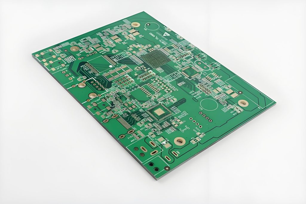
How Does FPC Adopt SMT Assembly Technology?
Process requirements for mounting SMDs on flexible printed circuit boards (FPC):
As electronic products continue to miniaturize, surface mount technology (SMT) has become the mainstream for a large number of consumer electronics. Driven by compact product designs and limited assembly space, mounting SMDs on FPCs has evolved into a key technological development trend. Below are the core process requirements and key considerations for SMD surface mounting on FPCs.
Conventional SMD Mounting
Features
Low mounting accuracy requirements, a small quantity of components to be mounted (mainly resistors and capacitors), or a small number of individual odd-form components.
Key Processes
- Solder Paste Printing: FPCs are positioned on dedicated pallets by their physical form for printing. Small semi-automatic printers are generally used for this step; manual printing is an alternative but yields lower quality than semi-automatic printing.
- Component Mounting: Manual mounting is feasible for most components; a manual placement machine can be used for individual components with relatively higher positional accuracy requirements.
- Welding: Reflow soldering is the standard process; spot welding may be adopted under special circumstances.
High-Precision SMD Mounting
Features
FPC substrates require dedicated positioning marks and must be kept flat—FPCs are inherently difficult to fix, making consistency hard to guarantee in mass production. This process also demands high-end manufacturing equipment, and poses greater challenges for controlling solder paste printing and component mounting processes.
Key Processes
- FPC Fixing: FPCs must be securely fixed on pallets throughout the entire process from solder paste printing and component mounting to reflow soldering, and the pallets used must have a low thermal expansion coefficient. Two fixing methods are available for selection based on actual production conditions: Method A for QFPs with a lead pitch of 0.65mm or above, and Method B for QFPs with a lead pitch below 0.65mm.
- Method A: Place the pallet on a positioning template, fix the FPC on the pallet with thin high-temperature resistant tape, then separate the pallet from the template for printing. The tape must have moderate adhesiveness, be easily peelable after reflow soldering, and leave no adhesive residue on the FPC.
- Method B: Use a custom-manufactured pallet that must minimize deformation after repeated thermal shocks. The pallet is fitted with T-shaped positioning pins, whose height is slightly higher than the FPC surface.
- Solder Paste Printing: Since FPCs are fixed on pallets (with positioning constraints) and high-temperature tape may cause unevenness between the FPC and pallet surfaces, an elastic scraper must be used for printing. The composition of solder paste significantly impacts printing results, so the appropriate type of solder paste must be selected. In addition, the printing template for Method B requires specialized processing.
- Mounting Equipment Requirements:
- First, the solder paste printer must be equipped with an optical positioning system; otherwise, welding quality will be severely compromised.
- Second, even when fixed on a pallet, tiny gaps will inevitably exist between the FPC and the pallet—this is the most notable difference from rigid PCBs. Equipment parameter settings have a major impact on printing results, mounting accuracy, and welding quality, so strict process control is essential for FPC component mounting.
Additional Key Step
To ensure assembly quality, it is recommended to dry FPCs before the mounting process.