Learn what tented vias are, how they work, key benefits, IPC standards, design rules, and best applications for high‑performance PCB manufacturing and assembly.
What Is a Tented Via in PCBs?
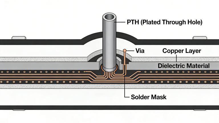
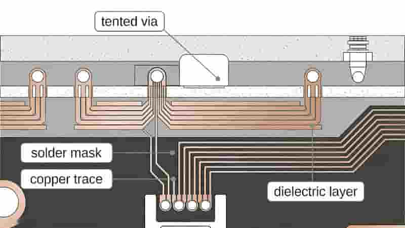
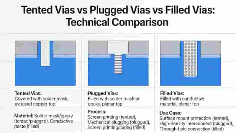
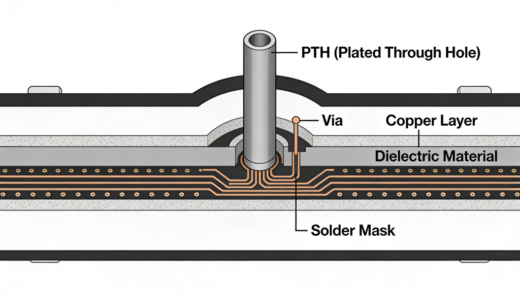
A tented via is a plated through‑hole (PTH), blind via, or buried via fully or partially covered with solder mask on one or both sides of a printed circuit board. The solder mask forms a protective “tent” over the via opening, sealing the hole while keeping the inner barrel conductive.
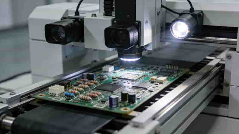
Unlike exposed vias, tented vias block solder wicking, contamination, and short circuits during SMT assembly and long‑term use. They are widely used in HDI, multilayer, and high‑speed PCB designs.
Types of Tented Vias (IPC Standards)
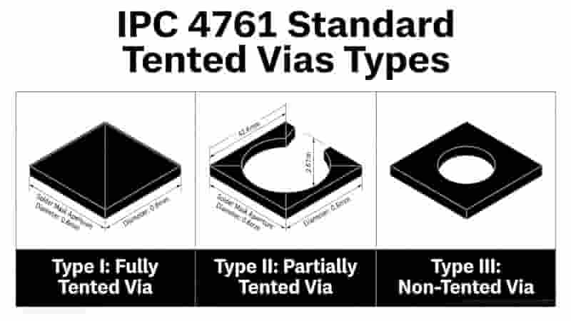
Tented vias follow IPC‑4761 and IPC‑4762 industry standards:
- IPC‑4761 Type 1a: One‑sided tenting (top or bottom)
- IPC‑4761 Type 1b: Two‑sided tenting (full coverage)
- IPC‑4762 Type 2a/2b: Tented with extra solder mask reinforcement
Key Benefits of Tented Vias
- Prevent solder bridging in fine‑pitch SMT and BGA assemblies
- Improve insulation and reduce signal leakage in high‑frequency boards
- Enable trace routing directly over vias in dense layouts
- Enhance PCB reliability by blocking moisture, dust, and oxidation
- Support EMI/EMC compliance in industrial and medical electronics
Ideal Applications for Tented Vias
Tented vias deliver the most value in these PCB designs:
- High‑density interconnect (HDI) PCBs
- Multilayer boards for industrial controls
- SMT‑heavy consumer and automotive electronics
- High‑speed communication and RF circuit boards
- Medical devices requiring high insulation and stability
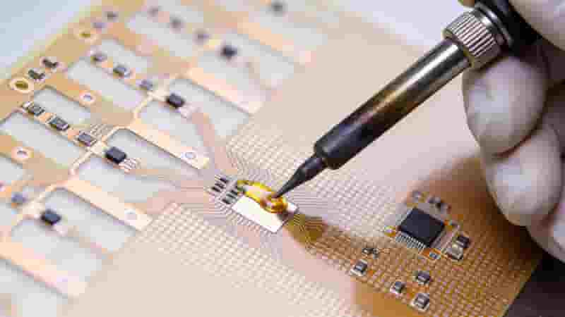
How Tented Vias Are Manufactured
Two industry‑standard processes create reliable tented vias:
1. Mask Tenting: Solder mask is retained over vias during the standard imaging process.
2. Paste Tenting: Special solder mask paste is printed directly onto via openings as a secondary step.
Solder mask thickness for tented vias is typically 10–30 microns to ensure proper curing and coverage.
Tented Via Design & DFM Rules
- Via diameter ≤ 0.3 mm (12 mil) for consistent tenting
- Minimum clearance ≥ 0.25 mm from SMT pads
- Avoid tenting vias used for test points or thermal dissipation
- Use LPI solder mask for uniform coverage
- Label tented vias clearly in Gerber and drill files
Conclusion
Tented vias are a cost‑effective, high‑reliability solution for modern PCB design. They improve assembly yield, electrical safety, and long‑term durability while supporting dense, high‑performance layouts. Following IPC standards and proper DFM rules ensures consistent, production‑ready results.
Need High‑Quality PCBs with Reliable Tented Vias?
Get professional PCB manufacturing, DFM analysis, and fast quotes for your custom projects.
Request a Free Quote
How to Solder On Flex PCB? Complete Professional Guide
Multilayer PCB Prototyping & Manufacturing Services | Fast & Reliable
Flexible PCB Manufacturer & Flex PCB Fabrication | Custom & Reliable

How to Find Reliable China PCB Manufacturers: 5 Critical Vetting Tips
What is the Difference Between PTH and Via in PCBs?