HDI PCB is an advanced printed circuit board technology for high‑component‑density electronics. This guide covers core HDI PCB layout principles, via design, trace rules, stackup, and IPC standards for engineers and buyers.
What Is HDI PCB Layout?
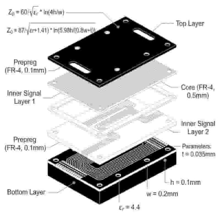
High Density Interconnects (HDI PCB) layout refers to advanced PCB design techniques used when trace widths drop below 8 mils (0.2 mm). These methods allow higher component density, smaller board size, and better performance for modern electronics like smartphones, industrial controllers, and networking devices.
Designers adopt HDI PCB layout when working with fine‑pitch BGAs, high pin counts, and miniaturized products. Unlike standard PCBs, HDI designs require special vias, thin traces, and strict routing rules to meet IPC standards and manufacturing requirements.
Key Features of HDI PCB Layout
A professional HDI PCB includes these critical features to support high‑density routing and reliable manufacturing:
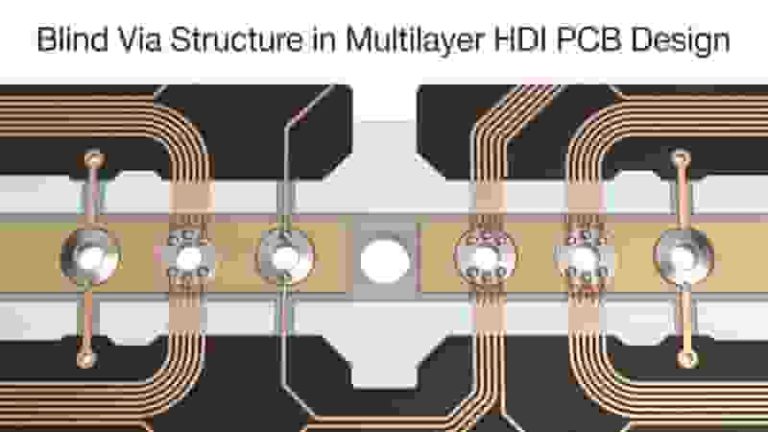
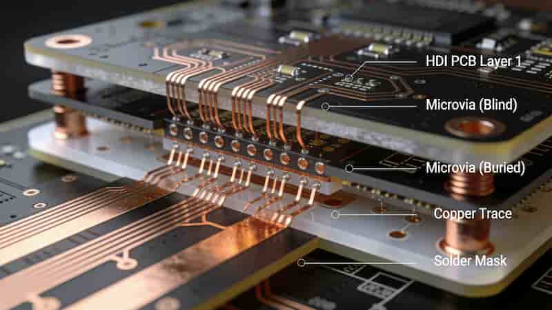
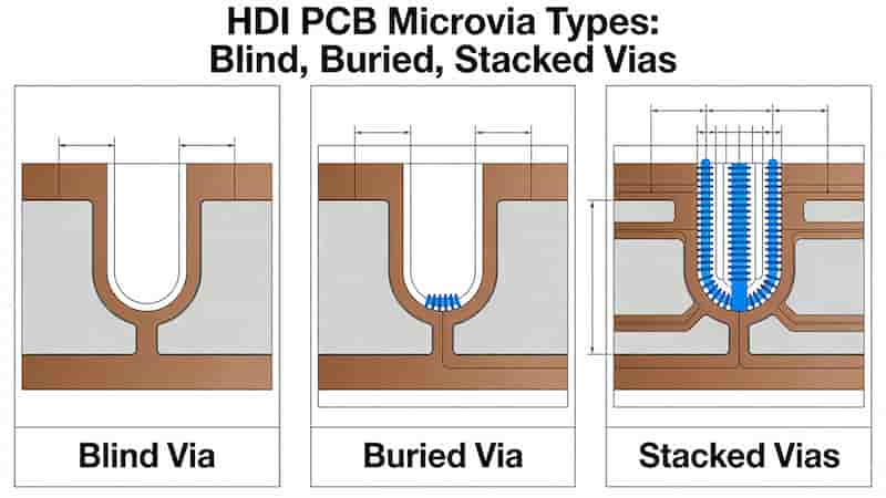
Smaller Microvias
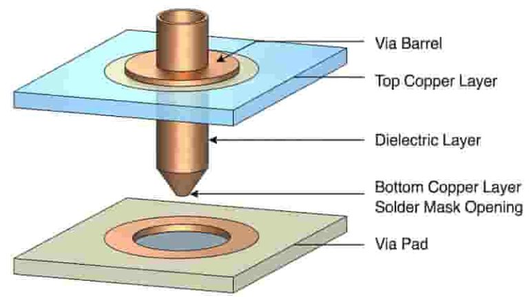
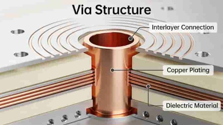
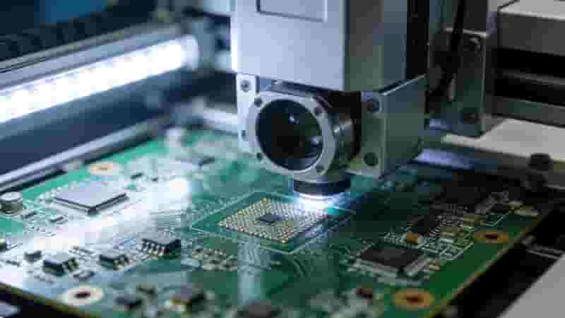
HDI boards use laser‑drilled microvias, blind vias, buried vias, and staggered vias. These vias have smaller aspect ratios and diameters than standard through‑hole vias, ideal for fine‑pitch components.
Thinner Traces
Thin traces in HDI PCB layout enable higher routing density and connections to small pads and in‑pad vias, which is essential for compact electronic designs.
Higher Layer Count
High‑performance HDI PCB can reach 20+ layers to support FPGAs, high‑speed processors, and complex industrial systems.
Low Signal & High‑Speed Design
HDI boards are optimized for low‑voltage, high‑speed signals, ensuring signal integrity and avoiding ESD or overheating issues.
Trace Sizes and Vias in HDI PCB Layout
Fine‑pitch components (0.5 mm, 0.75 mm, 0.8 mm BGAs) define trace and via rules in HDI PCB layout. We follow IPC‑2221A / IPC‑2222 standards to ensure manufacturability and yield.
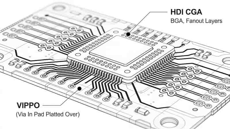
Through‑hole vias have a maximum aspect ratio of 8:1. For smaller vias, microvias and stacked vias become necessary. Dog‑bone fanout and VIPPO (in‑pad vias) are widely used for BGA routing.
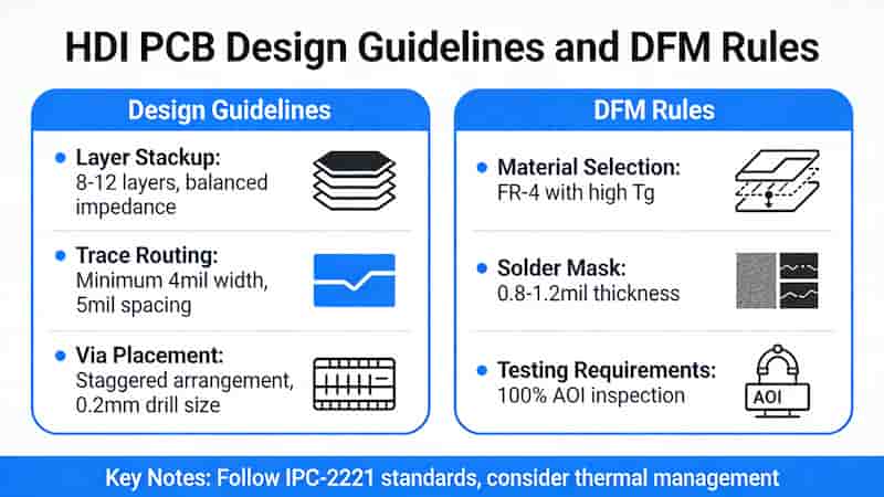
Basic HDI Design Guidelines
These proven HDI PCB layout guidelines help engineers achieve reliable, cost‑effective, and mass‑producible designs:
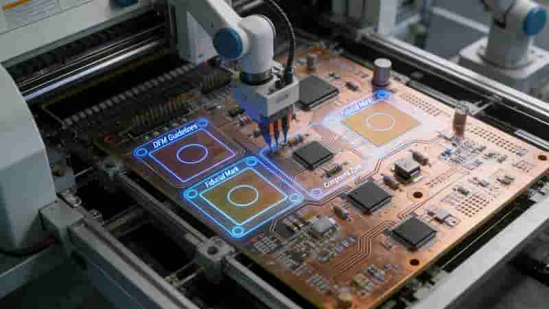
1. Confirm Manufacturer Capabilities
Always verify fabrication capabilities before finalizing HDI PCB design, including minimum trace, via, and layer limits.
2. Control Trace & Pad Clearance
Follow DFM rules for spacing, solder mask clearance, and impedance control to avoid manufacturing failures.
3. Avoid Unnecessary Vias & Layers
Skip staggered vias or ELIC structures unless required. Fewer layers reduce cost and lead time for HDI PCB projects.
4. Prioritize Signal Integrity
Use impedance‑controlled routing and high‑speed design principles to maintain stable performance in HDI PCB layout.
Standard PCB vs HDI PCB Comparison
| Item | Standard PCB | HDI PCB |
|---|---|---|
| Trace Width | ≥8 mils | ≤6 mils |
| Via Type | Through‑hole | Microvia, Blind, Buried |
| Density | Low to Medium | High |
| Application | General Electronics | High‑Tech, Miniature Products |
Summary
HDI PCB layout is a mandatory technology for modern high‑density electronic products. By following IPC standards, proper via design, trace control, and DFM guidelines, you can create reliable, compact, and high‑performance HDI PCB for industrial, medical, consumer, and communication applications.

Get Your HDI PCB Quote & Custom Solution
We provide professional HDI PCB design support, prototyping, mass production, and turnkey assembly services. Contact us today for a free quotation, DFM review, and customized HDI PCB layout solution.
Send your Gerber file or BOM list to get an instant response and competitive pricing!
What is FR-4 Material in PCB Fabrication? The Complete Professional Guide
SMT PCB Assembly Services for Prototypes & Production

Aluminum PCB Prototype: The Ultimate Guide for Engineers and Designers
10 Essential Tips for Optimizing PCB Design for Manufacturing
What Is Prototype PCB Assembly