Professional HDI PCB manufacturing with microvia, blind & buried vias, supporting up to 30 layers.
ISO & IATF certified, ideal for 5G, automotive, medical & high-speed electronics.
HDI PCB Manufacturing Capabilities
We provide full-service HDI PCB manufacturing with advanced laser drilling, sequential lamination, and precision fabrication.
Our capabilities cover rigid & rigid-flex HDI PCB designs with microvia, blind via, and buried via structures up to 30 layers.
| Parameter | Specification |
|---|---|
| Max Layer Count | Up to 30 layers |
| Min Trace/Space | 3/3 mil (0.075 mm) |
| Min Laser Microvia | 0.10 mm (4 mil) |
| Via Structures | Blind, buried, stacked, staggered, via-in-pad |
| Materials | High-Tg, low-loss, halogen-free laminates |
| Certifications | UL, ISO 9001, IATF 16949, RoHS |
Core HDI Technologies & Vias
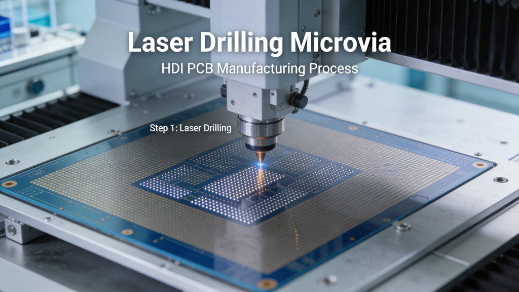
Microvia HDI boards rely on laser-drilled microvias to achieve higher wiring density and better signal integrity.
We support all standard via types for HDI PCB manufacturing:
- Blind Via: Connects outer layer to inner layer without penetrating the entire board
- Buried Via: Connects inner layers only, invisible from outer surfaces
- Microvia: Laser-drilled small via for high-density routing under fine-pitch BGAs
- Stacked & Staggered Vias: For ultra-high-density interconnect requirements
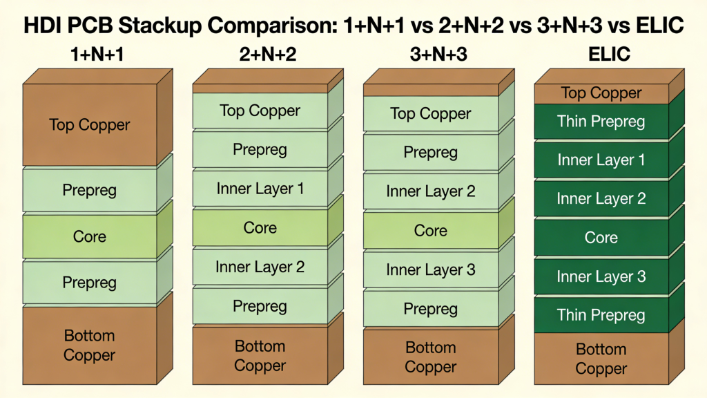
HDI Stackup Options
We offer full HDI PCB stackup solutions to match density, performance, and budget needs:
- 1+N+1 HDI: Cost-effective entry HDI for medium-density designs
- 2+N+2 & 3+N+3 HDI: High-density for fine-pitch BGAs & high-speed signals
- Any-Layer (ELIC) HDI: Maximum density for premium electronics
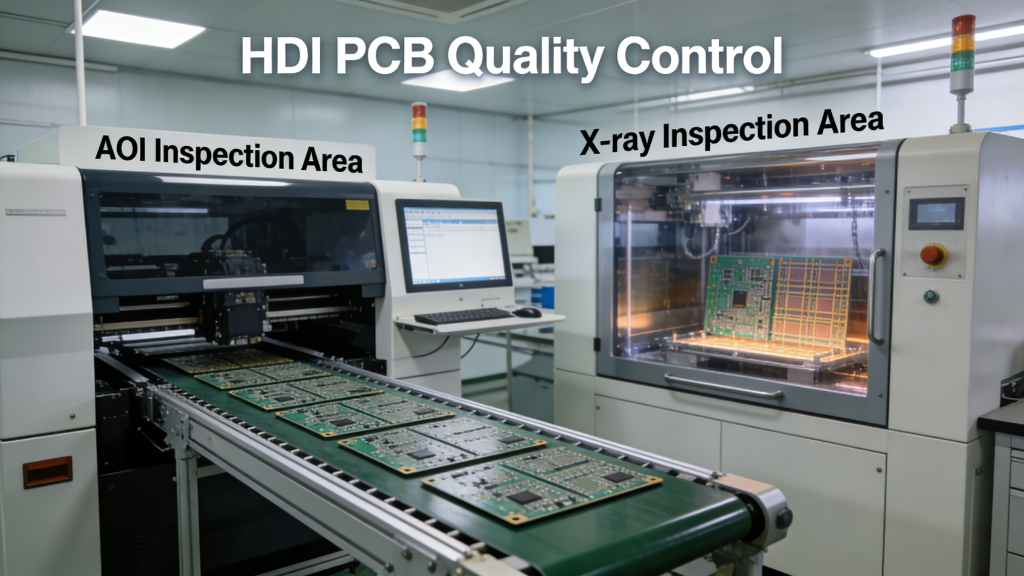
Quality Control & DFM Support
Every HDI PCB manufacturing order undergoes strict quality control to ensure reliability:
- AOI & X-ray inspection for microvias and fine circuits
- Electrical testing & impedance verification
- Micro-section analysis for structural validation
- Free DFM review for all HDI PCB designs
HDI PCB Cost & Lead Time
Cost depends on stackup complexity, layer count, materials, and quantity.
We provide transparent pricing for HDI PCB manufacturing:
- Prototype lead time: 5–8 working days
- Mass production: 10–15 working days
- Expedited service available for urgent projects
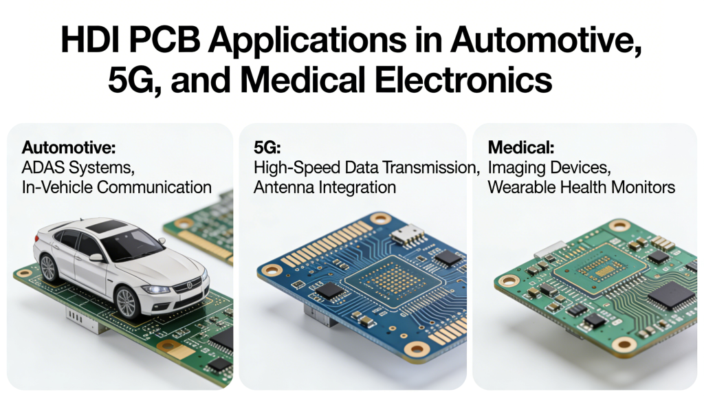
Applications & Industries
Our HDI PCB serves high-end industries worldwide:
- Automotive & EV electronics (ADAS, ECU, infotainment)
- 5G & telecom networking equipment
- Medical devices & portable diagnostics
- Consumer electronics & wearables
- Industrial IoT & automation systems
HDI PCB FAQs
Q: What is HDI PCB Manufacturing?
A: HDI PCB manufacturing produces high-density interconnect boards with microvias, fine lines, and thin materials for compact, high-performance electronics.
Q: What is the maximum layer count for your HDI PCBs?
A: We support 30-layer HDI PCB with blind, buried, and microvia structures.
Q: Do you provide DFM support for HDI designs?
A: Yes, we offer free HDI-focused DFM review to optimize yield and reliability.
Q: What certifications do you hold?
A: UL, ISO 9001, IATF 16949, RoHS compliant for global market access.
Summary
We are a trusted partner for professional HDI PCB manufacturing, delivering reliable microvia, blind & buried via HDI PCB up to 30 layers.
With strict quality control, full certifications, and expert DFM support, we help global engineers and buyers build high-performance electronic products.
Request Your HDI PCB Quote
Get a fast, free quote for your HDI PCB manufacturing project.
Upload Gerber files and specifications for 24-hour engineering review and pricing.
Get HDI PCB Quote
No MOQ for prototypes | Secure file upload | Global delivery
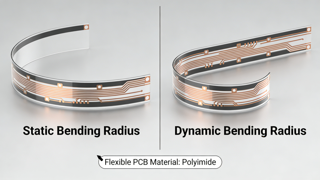
Single-Sided Flexible PCB Design Guide: Bending Radius, Trace Routing and Stiffeners
Professional LED PCB Manufacturing & Assembly Services
Flying Probe Testing for PCB: The Complete Professional Guide
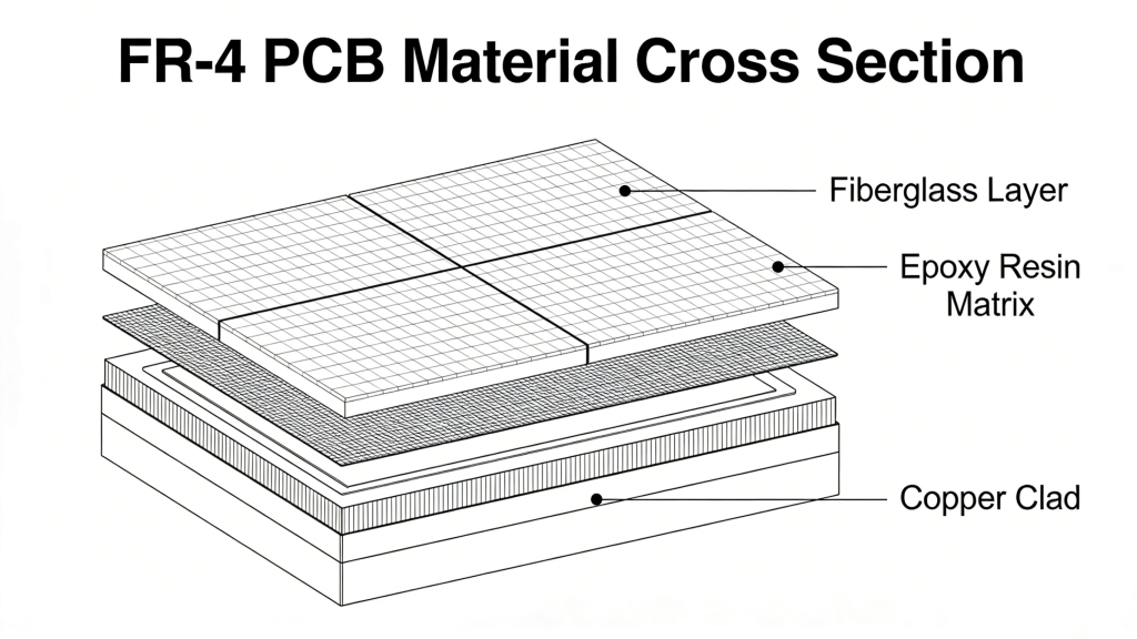
Why Choose FR-4 PCBs in 2025? Benefits, Applications & Custom Solutions for 5G, IoT & EVs
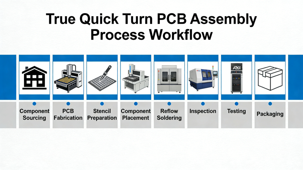
Quick Turn PCB Assembly in USA: The Strategic Guide to Speed, Cost & Reliability