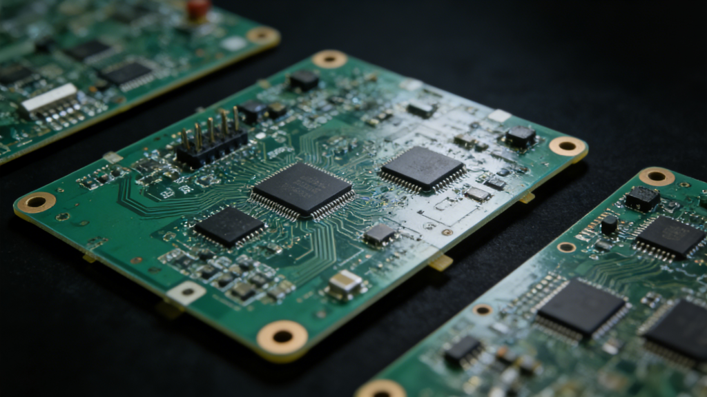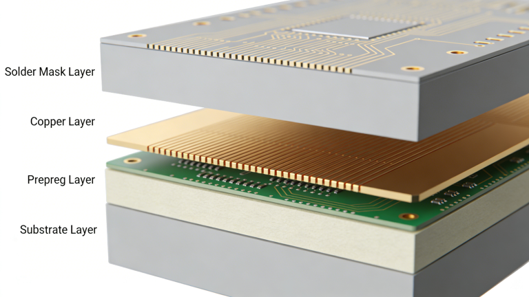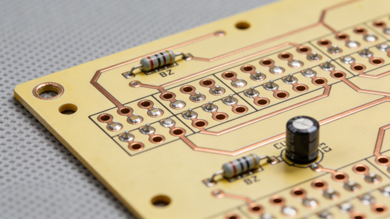
Standard PCB thickness is critical for mechanical strength, signal integrity, and assembly compatibility. This guide covers definitions, industry standards, influencing factors, manufacturing constraints, and design best practices for global industrial buyers.
What Is Standard PCB Thickness
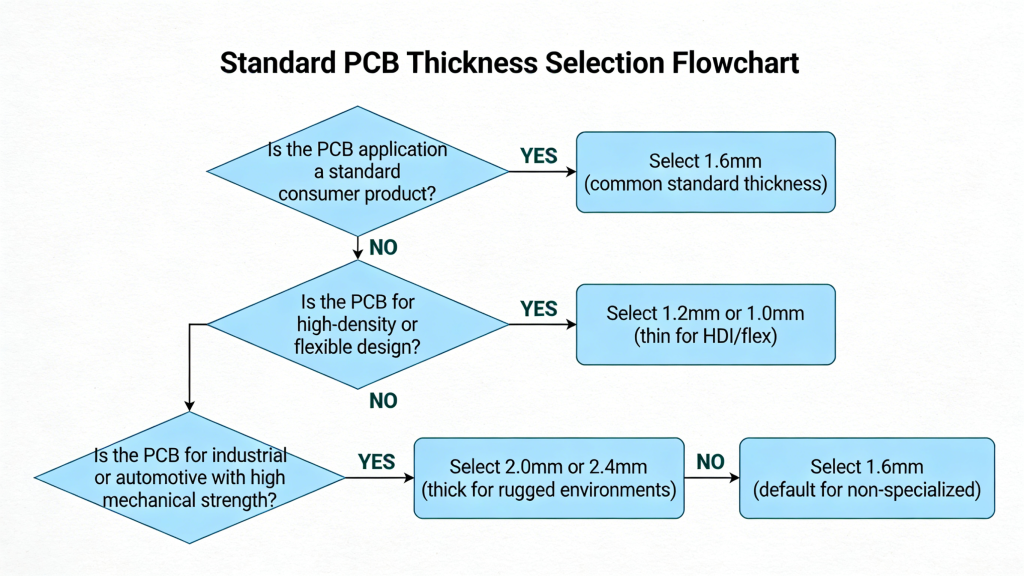
The global standard PCB thickness is 1.57 mm (0.062 in), commonly referenced as 1.6 mm for simplicity. This is the most widely used dimension for mainstream printed circuit boards.
Common industry thickness range includes:
- 0.78 mm (0.031 in) – Thin boards for compact electronics
- 1.6 mm (0.062 in) – Universal standard PCB thickness
- 2.36 mm (0.093 in) – Thick boards for industrial applications
Standard PCB thickness directly impacts durability, weight, performance, reliability, and assembly quality. All custom or standard boards must pass strict quality testing before mass production.
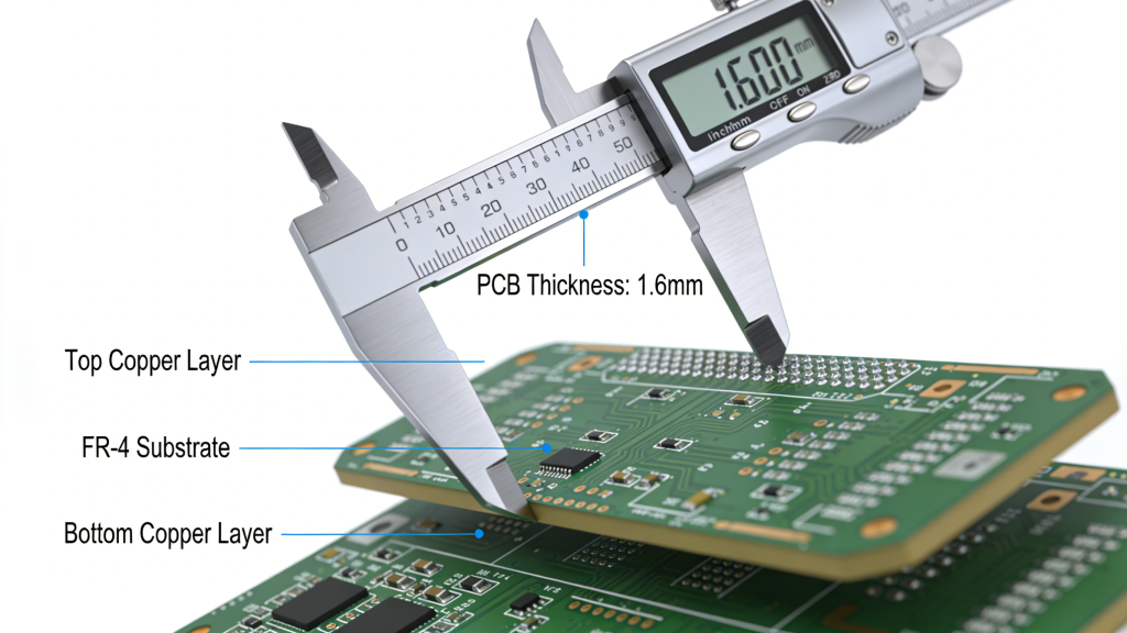
Key Factors Affecting Standard PCB Thickness
1. Copper Thickness
Standard copper thickness ranges from 1.4 to 2.8 mils (1-2 oz), determined by current-carrying requirements. Thicker copper increases material cost and processing complexity, directly influencing final board thickness.
2. Substrate Material
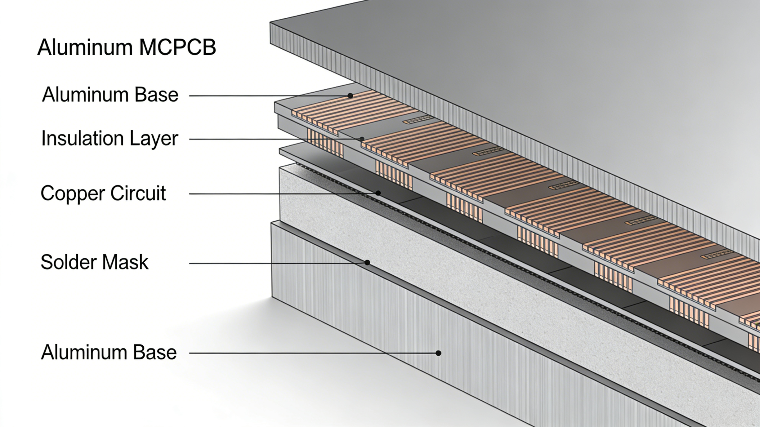
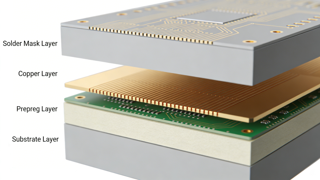
Substrate (dielectric core) is the non-conductive base of PCB. Common materials: FR-4, FR-1 thru FR-6, G-10/G-11, IMS. Material type, Tg value, and laminate thickness define the baseline of standard PCB thickness.
3. Number of PCB Layers
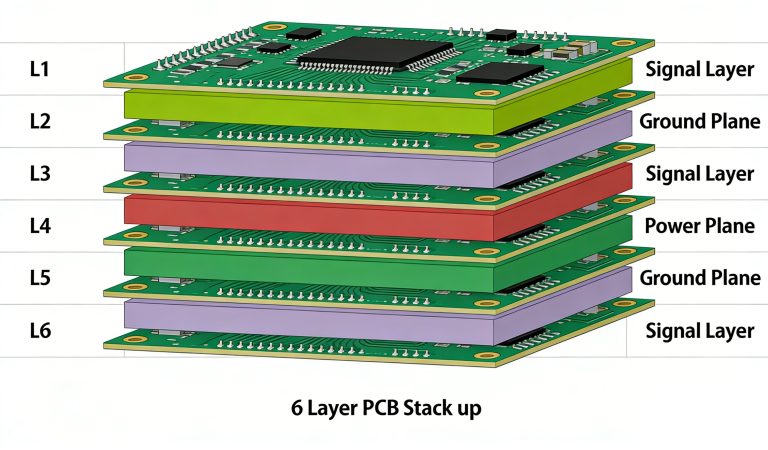
Layer count directly determines thickness:
- 2-6 layers: typically fits standard PCB thickness
- 8+ layers: often exceeds standard thickness
Overly thin layers for high-layer-count boards cause reliability risks. Maintain reasonable thickness for functional stability.
4. Signal Type
High-power signals require thicker boards with wider copper traces. Signal characteristics directly affect required standard PCB thickness or custom dimensions.
5. Through Hole / Via Types
Through vias, micro vias, blind vias, buried vias, and via-in-pad affect aspect ratio and stacking. High via density often requires adjusted thickness for stable manufacturing.
6. Operating Environment
Harsh environments (vibration, high temperature, humidity) need thicker boards for mechanical strength and stability. Connector compatibility also depends on consistent standard PCB thickness.
Manufacturing Factors Affecting Standard PCB Thickness
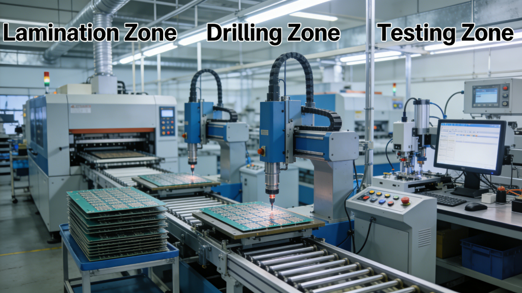
1. Drilling Equipment Capability
Standard drilling aspect ratio is 7:1 (depth:diameter). Exceeding this ratio requires special equipment, increases cost, and may limit thickness options.
2. Copper Plating & Etching
Inner layer copper thickness affects lamination uniformity. Thick copper changes overall thickness and requires controlled manufacturing processes.
3. Layer Stack-Up & Lamination
More layers make it harder to maintain standard PCB thickness. Forcing thin cores for high layer counts reduces reliability and increases production failure rate.
Design Considerations for Non-Standard PCB Thickness
When deviating from standard PCB thickness, consider these factors:
1. Factory Production Capability
We support PCB thickness from 0.3 mm to 3.0 mm, covering standard and most non-standard requirements with stable mass production.
2. Additional Cost & Lead Time
Non-standard thickness usually increases cost and lead time. Compare standard vs. custom total cost before final design.
3. Assembly Compatibility
Ensure connectors, sockets, and assembly equipment support non-standard thickness to avoid mating or mounting issues.
Standard PCB Thickness Comparison Table
| Thickness (mm) | Typical Layer Count | Main Applications | Status |
|---|---|---|---|
| 0.8 | 2-4 | Compact electronics, IoT | Common thin type |
| 1.0 | 2-4 | Handheld devices | Standard range |
| 1.6 | 2-6 | General electronics, industrial | Standard PCB thickness |
| 2.0 | 6-10 | Power, automotive | Thick type |
| 2.4+ | 10+ | Backplane, heavy industry | Custom thick |
Conclusion
Standard PCB thickness (1.6 mm) is the most cost-effective and reliable choice for most projects. Thickness is determined by layer count, copper, substrate, signal type, vias, environment, and manufacturing limits.
We provide full support for standard PCB thickness and custom thickness from 0.3 mm to 3.0 mm, with ISO, UL, RoHS compliance, stable quality, and global export service.
Get Your Standard PCB Thickness Quote Now
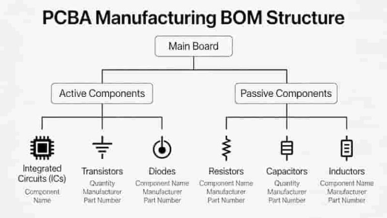
Send Gerber files and BOM for a fast, free quotation. We support standard and custom PCB thickness with fast lead times and 100% quality assurance.
Request Free Quote

Rapid PCB Prototyping | Fast-Turn PCB Fabrication Services
4 Layer PCB Manufacturing & Prototype Service | Factory Direct FR4 Stackup
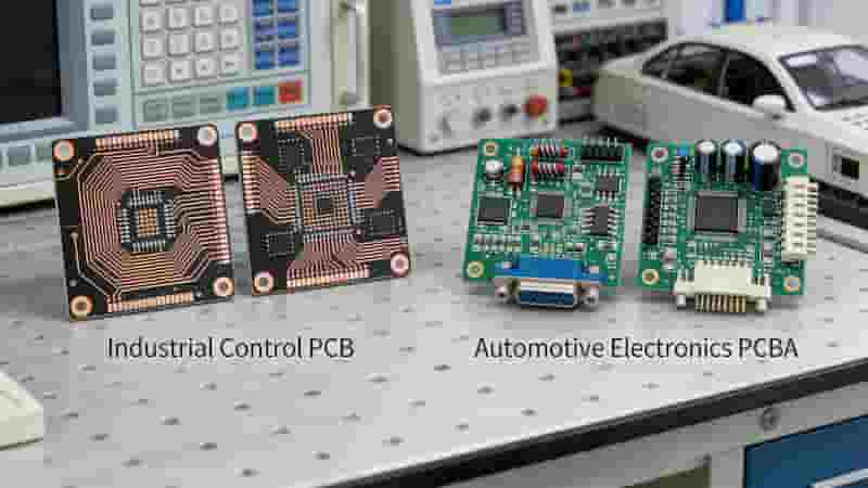
What Is the Difference Between PCB and PCBA? A Complete Guide for Industrial Buyers

Why Choose Us for Double Sided PCBs?
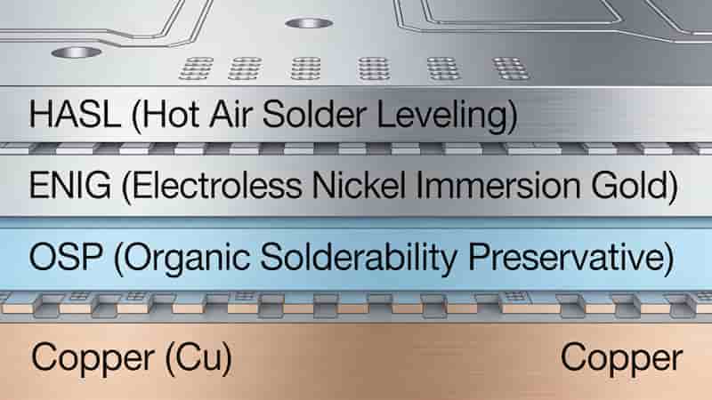
Best PCB Surface Finish: How to Choose the Right Type for Your Project in 2025