Learn what prototype PCB assembly is, why it matters, types, process steps, cost factors, and how to choose a reliable partner. We provide fast‑turn, high‑quality prototype PCB assembly for global customers.
Prototype PCB Assembly Guide: Process, Types, Cost & Partner Selection
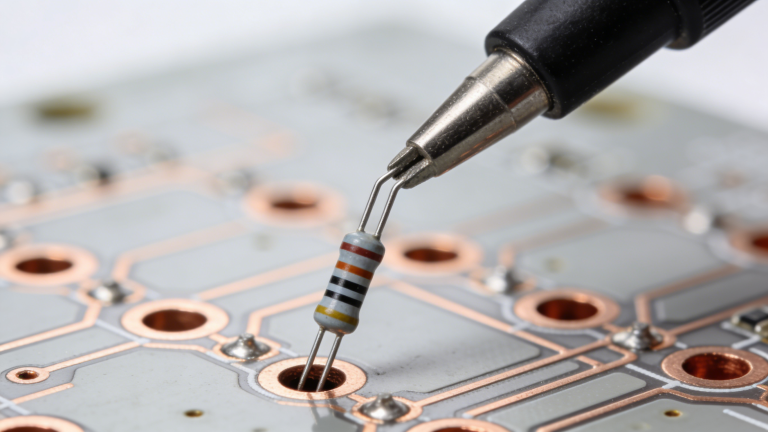
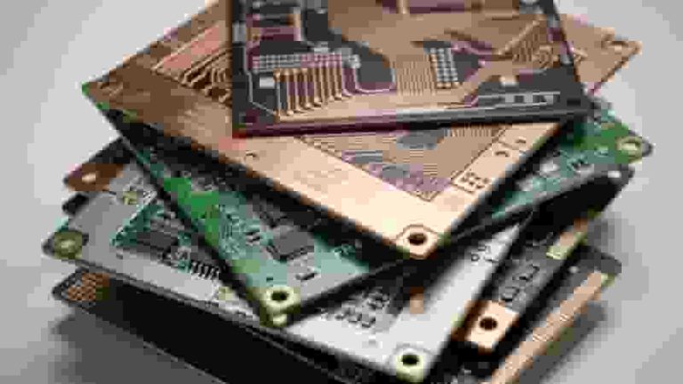
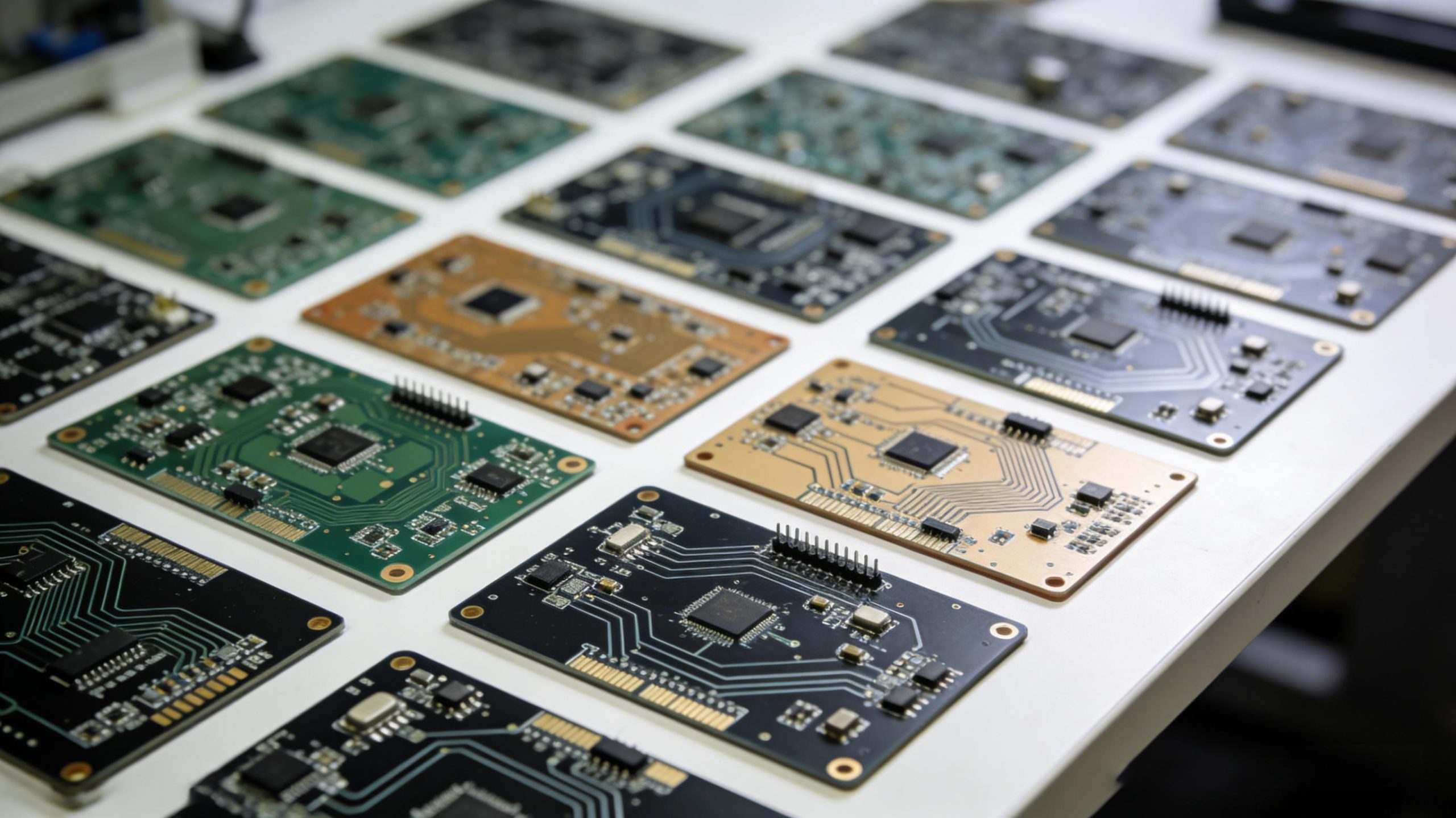
A printed circuit board prototype refers to the initial version of a printed circuit board design that is fabricated for concept verification and testing. As one of the most crucial steps in electronics product development, building a prototype PCB provides the first physical form of the circuit schematics to examine functionality, analyze signal integrity, and evaluate manufacturability before high‑volume production. This process is also known as prototype PCB assembly.
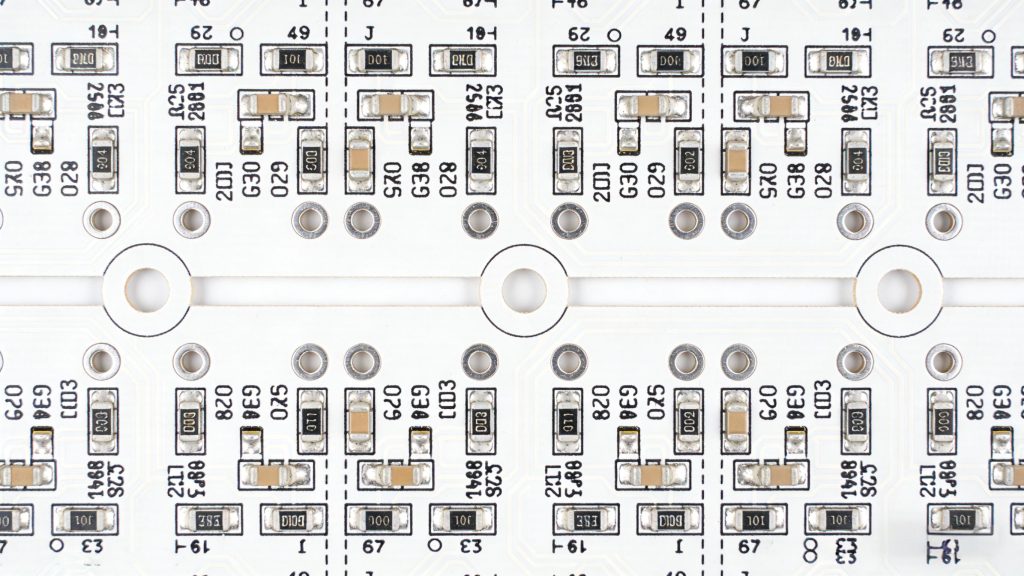
In essence, PCB prototype assembly enables developers and engineers to convert electronic designs into tangible boards with components soldered on them. It bridges the gap between theoretical schematics and mass manufacturing, providing key insights and optimization opportunities early in the cycle. Both the fabrication and assembly processes are critical for prototype construction. While PCB fabrication focuses on turning CAD designs into physical boards, prototype PCB assembly is the process of soldering electronic components onto those boards based on bill of materials (BOM) requirements to build functioning prototypes.
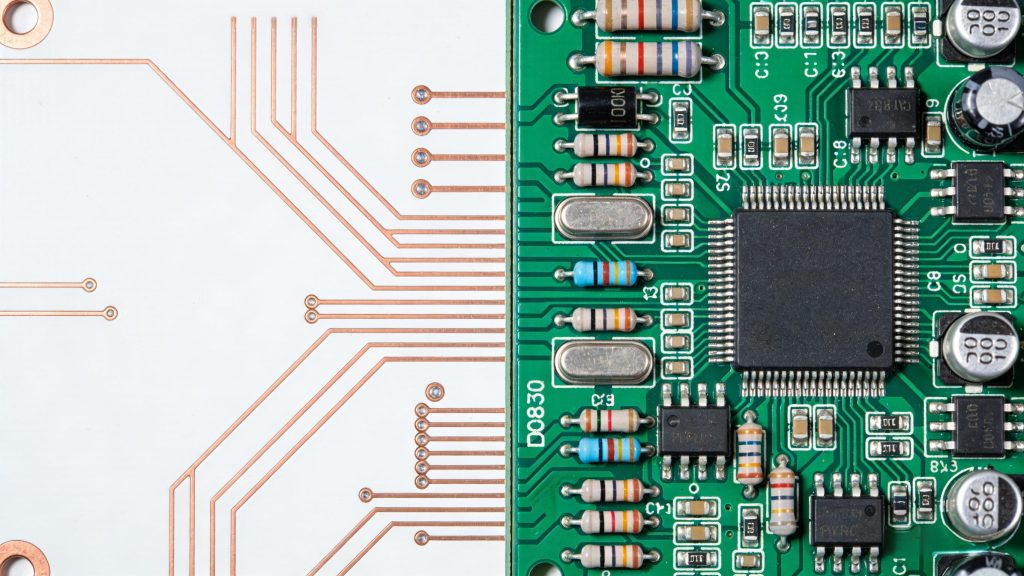
As proof of design concept and part of product development cycle, prototype PCB assembly offers electronics companies and innovators the chance to de‑risk technological and manufacturing uncertainties at relatively low cost and lead time. It is an indispensable step to validate functionality, safety and performance metrics before ramping up production with bulk orders. Hence, choosing a qualified prototype assembly partner bears significant impact on ultimate product success.
Why Use Prototype PCB Assembly?
There are several key reasons why investing in professional prototype PCB assembly services is worthwhile for most electronics hardware companies and developers today:
- Verify design functionality and concepts: The number one goal of building prototype boards is examining the real‑world functionality and performance of electronic designs. By putting schematics into testable boards, prototype assembly enables validation of design correctness and detection of potential flaws that may compromise functionality. This verification process mitigates risks prior to large‑scale manufacturing.
- Accelerate product development and time‑to‑market: Through early verification and problem discovery, quality PCB prototype assembly helps compress development cycles significantly. Rather than finding issues after production investment, prototyping offers an efficient and low‑cost approach to optimizing and finalizing designs, saving overall engineering time by over 60% according to research.
- Facilitate demonstration, marketing and funding: An assembled PCB prototype lets innovators demonstrate product viability and technology capacity to secure marketing leads, early adopters and investor funding ahead of production. For hardware startups, an impressive prototype builds business case for securing the financing to proceed further.
- Refine designs for manufacturability: By reflecting real‑world manufacturing processes more closely, prototype assembly finds design for manufacturability (DFM) issues as well design flaws to optimize. This lessens surprises down the line, and leads to more efficient transition from prototyping to mass production.
In essence, investing in professional PCB prototype assembly services creates remarkable value. It transforms designs from ideas to functioning boards efficiently, enabling concept validation, performance verification, design refinements, demonstration exhibits, and business case shaping before large‑scale manufacturing commitments.
Types of Prototype PCB Assembly
There are several key categories and techniques for assembling electronic components onto PCB prototypes which cater to different production needs:
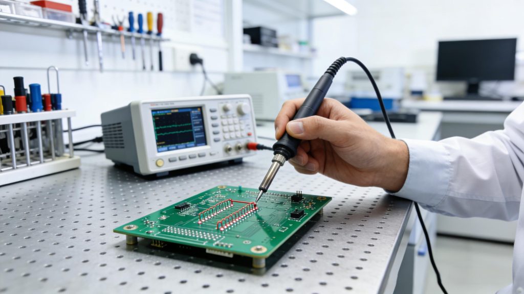
Manual Assembly vs Automated SMT Assembly
The simplest prototype PCB assembly uses manual soldering of components by technicians, suitable for very low volume or limited quantity orders. However automated surface mount technology assembly offers higher efficiency, consistency and manufacturability for complex board productions.
Through‑Hole vs SMT Assembly
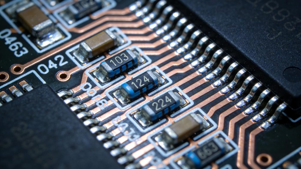
While through‑hole components have connector pins for passing through holes in boards, SMT or surface‑mount components get directly soldered onto surface pads. Both through‑hole assembly (THA) and SMT assembly have respective applications. Advanced tech allows mixing THA parts on primarily SMT boards.
Single‑sided vs Double‑sided Assembly
How components are placed and soldered on a PCB depends much on the design – from plain single‑sided prototype PCB assembly to more complex double‑sided assembly which solders parts on both sides of boards and enables higher component density overall.
Hybrid Assembly Techniques
With state‑of‑the‑art manufacturing capabilities, leading prototype assembly services allow component mixtures on boards, say combining 0201 size tiny chips along with larger SMT parts and some through‑hole passives on double‑side boards for optimized productions. Such hybrid assembly provides the needed flexibility.
In summary, professional prototype PCB assembly partners offer a spectrum of verified assembly processes catering from simple manual builds to advanced automated mixed productions in both low to medium quantities, providing the right solution for customers’ prototyping needs prior to mass manufacturing orders.
Prototype Assembly Types Comparison
| Assembly Type | Method | Best For | Key Advantage |
|---|---|---|---|
| Manual Assembly | Hand soldering by technicians | Very low volume, simple boards | Low setup cost, flexible revisions |
| Automated SMT Assembly | Pick-and-place + reflow soldering | Medium to high volume, complex boards | High consistency, fast throughput |
| Through-Hole Assembly | Leaded components inserted through holes | High-power components, connectors | Strong mechanical bond |
| SMT Assembly | Components soldered onto surface pads | Compact, high-density designs | Small footprint, excellent high-frequency performance |
| Single-sided Assembly | Components on one side only | Simple, low-cost designs | Simplified manufacturing, lower cost |
| Double-sided Assembly | Components on both sides | Space-constrained, high-density designs | Maximizes board space utilization |
| Hybrid Assembly | Mix of SMT, through-hole, and various sizes | Complex boards with diverse components | Maximum design flexibility |
Prototype PCB Assembly Process Steps
The professional process of assembling prototype PCBs, whether utilizing automated SMT lines or manual assembly, generally follows standardized assembly stages to actualize CAD designs into functioning boards:
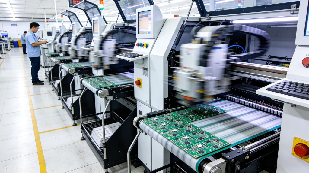
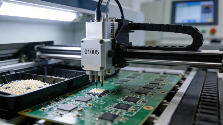
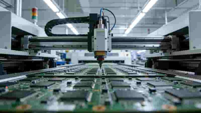
- SMT Pick‑and‑Place Stage: The core process uses advanced pick‑and‑place machines to selectively populate components onto circuit boards based on optimized programming and feeders setup. High precision and traceability is ensured during this mass component placement stage.
- SMT Reflow Soldering: After accurate component positioning, the boards pass through industrial reflow ovens for simultaneous precision soldering of SMT parts under carefully optimized thermal profiling to permanently attach parts to board surfaces.
- Cleaning/Washing: Once boards are reworked for any fixes, the assembly process proceeds to using cleaning solutions to thoroughly wash flux residues off board surfaces after soldering, ensuring ionic cleanliness.
- AOI and Functional Testing: Quality checks follow assembly stages – automated optical inspection checks component placement while rigorous functional testing examines board performance metrics to specification compliance using fixture testing among other methods before programming final firmware builds onto boards.
- Final Programming/Flashing: These downloads optimized software/firmware builds to boards through interfaces, completing the prototype PCB assembly for design validation before shipping to customers.
In summary, by following robust assembly protocols and quality management systems, professional PCB assembly partners deliver exceptionally functioning, reliable and clean prototype boards on short lead times.
Factors Affecting Lead Time & Cost
The lead time to obtain assembled PCB prototypes as well as the associated cost depend on a mix of factors related to design specifications and assembly requirements:
- Order Quantity and Batch Size: The production volume ordered has significant impact – lower order quantities generally mean higher NRE costs from the assembler, while having 3–5 boards per batch streamlines assembly processes and reduces costs somewhat.
- Degree of Assembly Complexity: The intricacy of component placements, density of parts along with challenges of achieving reliable solder joints for chosen parts also adds to assembly effort and costs. Slopes of advanced SMT parts on double‑sided boards increases complexity for instance.
- Test Requirements Scope: The extent of functional tests and quality assurance checks involved after assembly also affects labor efforts and thereby overall cost. In‑circuit tests, environmental stress screening along with conformance validation require additional investments.
- Component Sourcing Lead Times: Hard‑to‑source parts locally means longer procurement lead times, pushing out overall assembly timelines significantly. The sooner clients finalize their bill of materials with readily available parts, the quicker assembly progresses.
- Production Responsiveness: During prototyping, design changes occur as testing provides feedbacks. Hence choosing assemblers with quick‑turnaround manual assembly capabilities allows accommodating revisions swiftly.
Overall, PCB prototype assembly cost varies in the range of $100 to $5000 based on above criteria while lead times can span 5 days to 4 weeks depending on order specifics and assembler capacities.
Cost & Lead Time Influencing Factors Summary
| Factor | Impact on Cost | Impact on Lead Time | Optimization Tip |
|---|---|---|---|
| Order Quantity | Higher volume reduces unit cost | May increase or decrease depending on setup | Order 3-5 boards per batch for best balance |
| Assembly Complexity | More complex = higher cost | Increases with density and double-sided designs | Simplify design where possible, consult DFM |
| Test Requirements | Adds labor and equipment cost | Additional testing adds hours to days | Define essential tests only for prototype stage |
| Component Sourcing | Rare parts cost more | Long lead times if parts are not in stock | Finalize BOM with readily available parts early |
| Production Responsiveness | Rush jobs may incur premium | Quick-turn services reduce waiting time | Choose partner with fast manual assembly capability |
Finding A Good Prototype Assembly Partner
Given the significant impacts of PCB prototype assembly quality on product development cycles, how to select the right assembly partner becomes extremely important. Here are key criteria companies should consider:
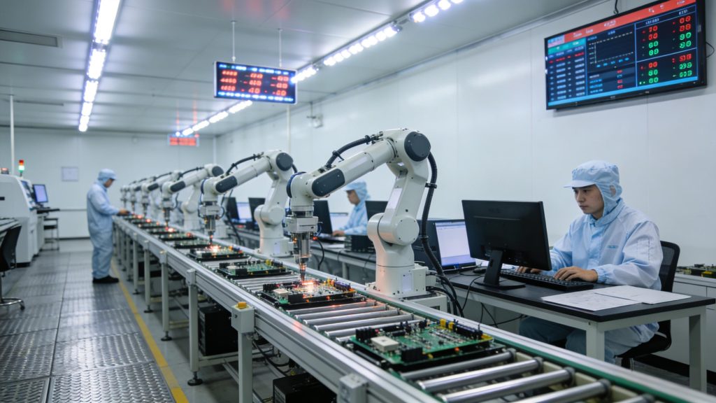
- Assembly Quality and Technical Capabilities: The foremost selection criteria is assessing partners’ technical capabilities across assembly techniques, production grade equipment, process controls and workmanship thresholds to meet quality and reliability requirements reliably.
- On‑Time Delivery Track Record: Analyzing past delivery timeliness for orders via metrics such as on‑time delivery rates offers insights into partners’ production bandwidths, responsiveness and capacities to meet lead time commitments despite inevitable prototype complexities.
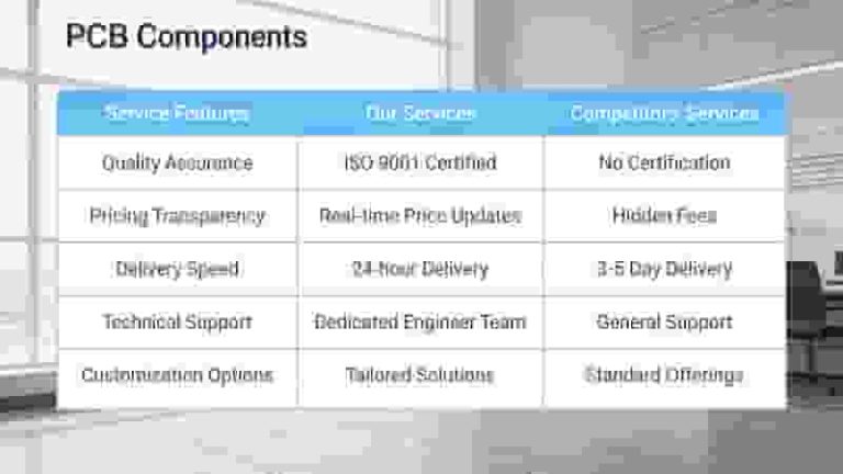
- Competitive and Transparent Pricing: Partners should offer clear assembly quotes benchmarked competitively against other prototype assemblers in alignment with capabilities, while outlining what service aspects influence costs to avoid hidden charges later. Reasonable pricing indicates good cost control abilities.
- Customer Service and Responsiveness: From assembly‑ready design reviews to post‑production support, partners’ consultation quality and uptime directly impacts collaboration effectiveness during prototyping rush jobs. Quick issue resolution indicates strong service competence.
In essence, aligning with PCB assembly partners with strong technical expertise, on‑time delivery records, pricing clarity and responsive support ensures high‑quality yet cost‑effective prototyping critical for new product introduction success.
Summary – Importance of Prototype PCB Assembly
In summary, prototype PCB assembly provides indispensable functional verification and concept validation capabilities for electronics product development teams through transforming design files into functioning boards with components soldered on accurately and reliably.
The assembly build quality directly impacts downstream processes from design optimizations to securing financing for productions. Hence quality considerations, balanced costs, responsive turnarounds and technical alignment are vital for companies to reap the most business value from the PCB assembly prototyping process while de‑risking technology uncertainties early.
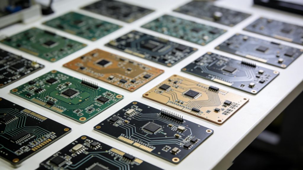
Along with fabrication partners, competent prototype assembly services reshape notions into testable boards rapidly to meet fast‑paced market dynamics, offering firms and innovators the competitive edges vital for commercial success. We specialize in professional turnkey PCB prototype assembly catering from concept verification builds to pilot productions, and have supported thousands of customers globally with exceptional quality deliveries and responsive support. Finding the right assembly partner makes all the difference in setting out innovation trajectories impactfully.
Related Reading
-
What is FR-4 Material in PCB Fabrication? The Complete Engineering Guide
FR-4 is the global industry-standard flame-retardant glass-reinforced epoxy laminate for rigid PCB fabrication. This guide explains definition, composition, properties, grades, selection, and why FR-4 PCB is the top choice for engineers and global buyers. What is FR-4 Material? FR-4 (Flame Retardant Type 4) is a NEMA-defined material grade for flame-resistant epoxy laminates. It is not…
-
What is FR-4 Material in PCB Fabrication? Complete Engineering Guide
FR-4 is the global industry-standard flame-retardant glass-reinforced epoxy laminate for rigid printed circuit boards. Defined by NEMA LI-1 and IPC-4101, it delivers balanced electrical insulation, mechanical strength, thermal stability, UL94 V-0 flame resistance, and cost efficiency for industrial, automotive, telecom, and consumer electronics. What is FR-4 Material? FR-4 (Flame Retardant Type 4) is a material…
-
What is a Surface Mount Device or SMD Component Package?
A Surface Mount Device (SMD) component package is a standardized enclosure designed for direct soldering onto PCB surfaces, enabling high-density assembly, miniaturization, and automated manufacturing in modern electronics. What Is an SMD Component Package? SMD stands for Surface Mount Device, referring to electronic components designed exclusively for Surface Mount Technology (SMT) assembly. An SMD component…
-
Turnkey PCB Assembly Services | Full & Partial Solutions
We provide end-to-end turnkey PCB assembly supporting full and partial models, with SMT assembly, THT, BGA/QFN, rigorous testing, and global logistics for industrial buyers, engineers, and importers. What Is Turnkey PCB Assembly Turnkey PCB assembly is a one-stop manufacturing solution covering PCB fabrication, component sourcing, assembly, testing, and delivery. We manage the full supply chain…
-
Through-hole PCB Assembly Service | IPC Certified THT PCBA Solutions
We provide reliable through-hole PCBAs assembly service for industrial, power, medical, aerospace and automotive applications. Our IPC-standard THT assembly supports prototypes to mass production with wave soldering, selective soldering and full inspection. Through-hole PCB Assembly Service Overview Our through-hole PCB assembly fulfills leaded assembly demands across industries. We deliver single-sided, double-sided and high-density multilayer through-hole…
-
Standard PCB Thickness: Complete Guide for Engineers & Buyers
Standard PCB thickness is critical for mechanical strength, signal integrity, and assembly compatibility. This guide covers definitions, industry standards, influencing factors, manufacturing constraints, and design best practices for global industrial buyers. What Is Standard PCB Thickness The global standard PCB thickness is 1.57 mm (0.062 in), commonly referenced as 1.6 mm for simplicity. This is…