Skip to content

Layer PCB

  • Home
  • Sample Page
Layer PCB
  • Engineering Teams Using Prototype PCB Assembly
    Uncategorized

    Prototype PCB Assembly Service – Fast, Reliable & Turnkey Solutions

    Byroot 2026-04-092026-04-09

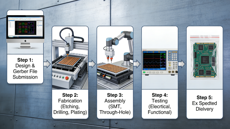
    Fast prototype PCB assembly with no minimum order quantity, flexible turnkey options and professional engineering support to help you validate designs quickly and reduce time-to-market. Turn your PCB design into fully assembled prototype boards in days, not weeks. We provide dedicated prototype PCB assembly services, combining PCB fabrication, component sourcing, SMT/THT assembly and testing into…

    Read More Prototype PCB Assembly Service – Fast, Reliable & Turnkey SolutionsContinue

  • PCB solder mask protection layer and insulation coating
    Uncategorized

    What Are PCB Boards Made Of? Complete Materials Guide for Engineers & Buyers

    Byroot 2026-04-092026-04-09

    Wondering what PCB boards are made of? This professional guide explains core PCB materials including substrates, copper foil, solder mask, surface finishes, and dielectric layers. We break down how each material impacts performance, reliability, thermal stability, and cost for industrial, automotive, medical, 5G, and high-speed electronic applications. Core Components of a PCB: What Are PCB…

    Read More What Are PCB Boards Made Of? Complete Materials Guide for Engineers & BuyersContinue

  • Flexible PCB structure and materials diagram
    Uncategorized

    16 Key Factors Affecting Flexible PCB Costs in 2025

    Byroot 2026-04-082026-04-08

    Understanding flexible PCB costs is essential for engineers, procurement teams, and manufacturers looking to control budgets while maintaining quality. This guide breaks down 16 critical factors that shape FPC pricing in 2025, including materials, layer count, manufacturing processes, order volume, and lead time. We also share practical cost‑saving strategies to help you optimize your next…

    Read More 16 Key Factors Affecting Flexible PCB Costs in 2025Continue

  • Uncategorized

    PCB Immersion Gold (ENIG) Surface Finish: Full Guide for Reliable Lead-Free PCBs

    Byroot 2026-04-082026-04-08

    PCB Immersion Gold (ENIG) is a premium surface finish delivering excellent solderability, oxidation resistance, and flatness for high-reliability printed circuit boards. This guide explains definition, benefits, process, pros & cons, comparisons, and applications for engineers and global buyers. What Is PCB Immersion Gold (ENIG) Surface Finish? PCB Immersion Gold (ENIG) (Electroless Nickel Immersion Gold) is…

    Read More PCB Immersion Gold (ENIG) Surface Finish: Full Guide for Reliable Lead-Free PCBsContinue

  • Uncategorized

    PCB Pad Design Basics: Standards, Rules & Best Practices for Engineers

    Byroot 2026-04-082026-04-08

    This guide covers core PCB pad design principles, component spacing, IPC standards, SMD/through-hole rules, thermal management, and DFM to boost assembly yield, reliability, and performance for industrial and export-grade PCBs. PCB Component Layout & Spacing Rules When laying out PCB components, designers must balance minimum component spacing against component height and thickness. Proper spacing prevents…

    Read More PCB Pad Design Basics: Standards, Rules & Best Practices for EngineersContinue

  • Expedited PCB manufacturing process for quick turnaround production
    Uncategorized

    Expedited PCB Services – Fast Turnaround for Urgent Prototypes & Production

    Byroot 2026-04-082026-04-08

    Expedited PCB services deliver fast circuit board prototyping, manufacturing, and assembly for global engineers and procurement teams. We provide high‑quality rush PCB solutions with reliable lead times, strict quality control, and competitive pricing for urgent export orders. Why Choose Expedited PCB Services In the global electronics industry, speed directly impacts time‑to‑market and project success. Expedited…

    Read More Expedited PCB Services – Fast Turnaround for Urgent Prototypes & ProductionContinue

  • Affordable PCB Prototyping Benefits for Engineers and Startups
    Uncategorized

    Why Choose Affordable PCB Prototyping?

    Byroot 2026-04-082026-04-08

    Affordable PCB prototyping helps engineers, startups and manufacturers validate designs quickly, cut development costs, avoid mass-production risks and speed up time-to-market without sacrificing quality or reliability. Key Benefits of Affordable PCB Prototyping Choosing affordable PCB prototyping brings measurable business and engineering advantages for every electronics project. Reduce Total Development CostEarly validation with low-cost PCB prototype…

    Read More Why Choose Affordable PCB Prototyping?Continue

  • Gold Finger PCB Edge Connector Plating Overview
    Uncategorized

    Gold Finger PCB Fabrication & Manufacturing Service

    Byroot 2026-04-082026-04-08

    Professional Gold Finger PCB manufacturing with IPC standards, hard gold plating, precision beveling, and reliable quality for industrial connectors, memory modules, and high-reliability electronics. Gold Finger PCB Guide – Quick Navigation What is a Gold Finger PCB? Gold fingers are the gold-plated edge connectors along the side of many PCBs, such as memory cards, graphics…

    Read More Gold Finger PCB Fabrication & Manufacturing ServiceContinue

  • LED Grow Light PCB Aluminum Core Circuit Board for Horticulture Lighting
    Uncategorized

    LED Grow Light PCB: Custom Aluminum PCB & Assembly for Horticulture Lighting

    Byroot 2026-04-082026-04-08

    Custom LED grow light PCB solutions with high-thermal aluminum substrates, full-spectrum design support, and turnkey PCB assembly for commercial indoor farming, greenhouses, and horticultural lighting systems. What Are LED Grow Lights? LED grow lights are artificial lighting systems engineered to emit optimized light spectra for plant photosynthesis. They replace or supplement natural sunlight for indoor…

    Read More LED Grow Light PCB: Custom Aluminum PCB & Assembly for Horticulture LightingContinue

  • PCB Copper Thickness Conversion oz to mm and mils
    Uncategorized

    PCB Copper Thickness Capabilities | Standard & Heavy Copper (0.5oz to 15oz)

    Byroot 2026-04-082026-04-08

    Learn about PCB copper thickness (copper weight), a critical parameter for current capacity, impedance control, and thermal performance. We specialize in heavy copper PCBs from 0.5oz to 6oz and up to 15oz for high‑power applications, delivering superior heat dissipation and lower resistance. What is PCB Copper Thickness? PCB copper thickness, also called PCB copper weight,…

    Read More PCB Copper Thickness Capabilities | Standard & Heavy Copper (0.5oz to 15oz)Continue

Page navigation

Previous PagePrevious 1 2 3 4 5 … 11 Next PageNext

© 2026 Layer PCB - WordPress Theme by Kadence WP

  • Home
  • Sample Page