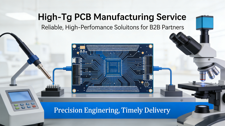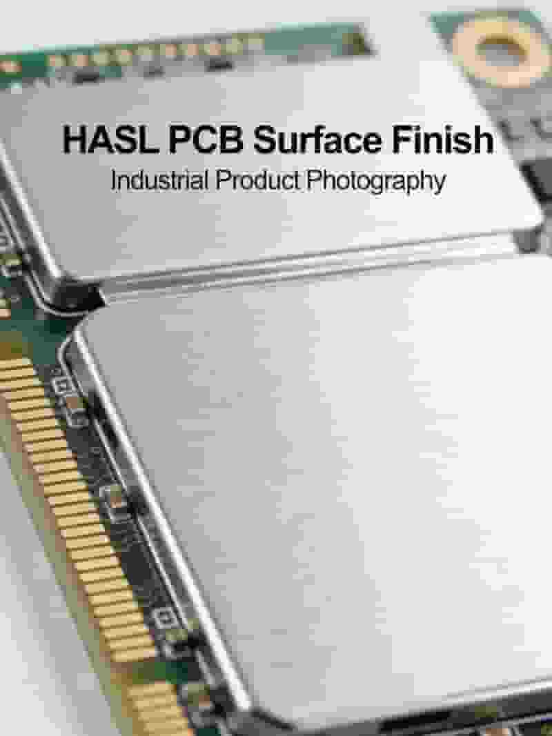
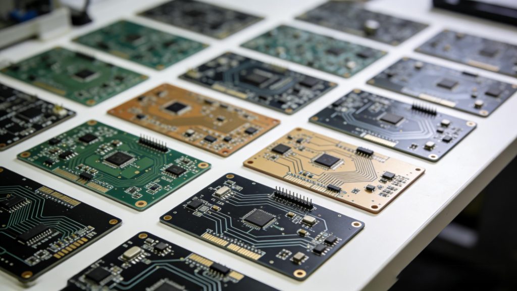
HASL (Hot Air Solder Leveling) is one of the most widely used and cost‑effective PCB surface finish processes in electronics manufacturing. It provides excellent solderability, protects copper from oxidation, and supports reliable assembly for through‑hole and standard SMT applications. This guide explains the HASL process, benefits, limitations, lead‑free options, and comparisons to help you select the best surface finish for your PCB project.
What Is HASL (Hot Air Solder Leveling)
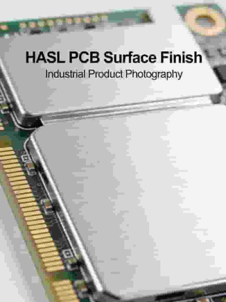
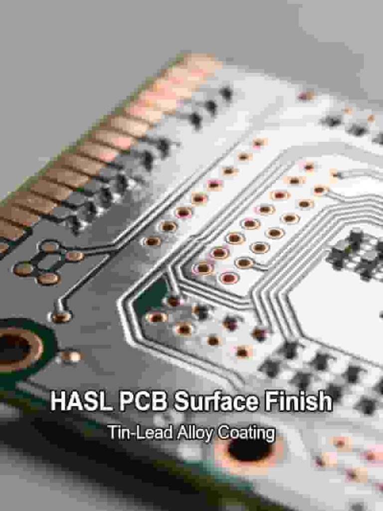
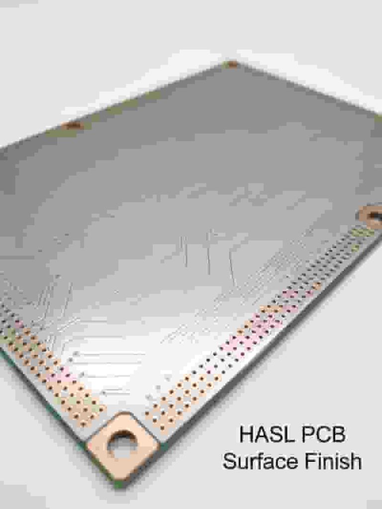
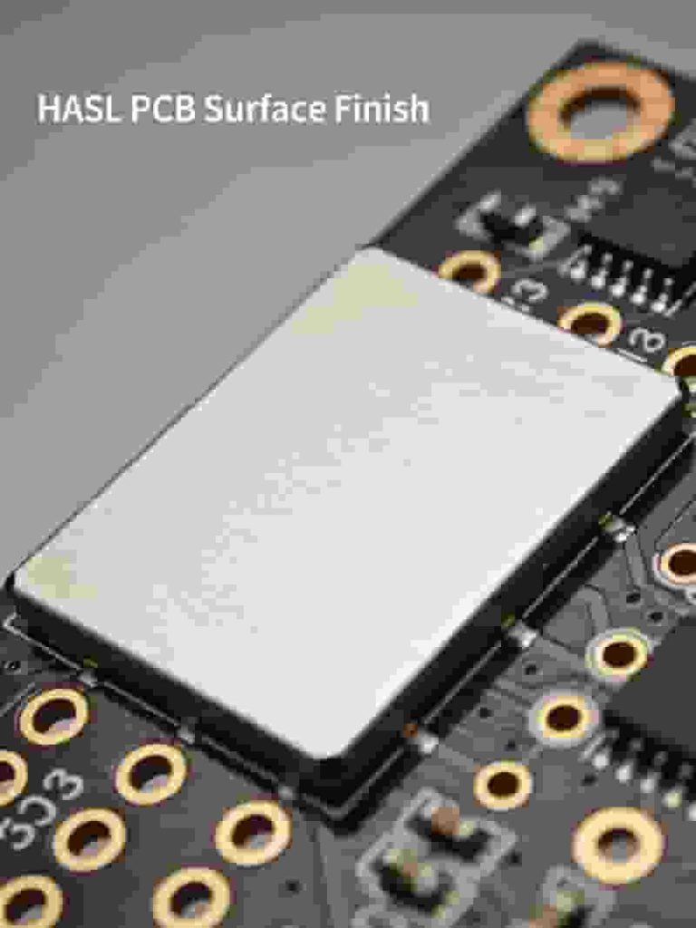
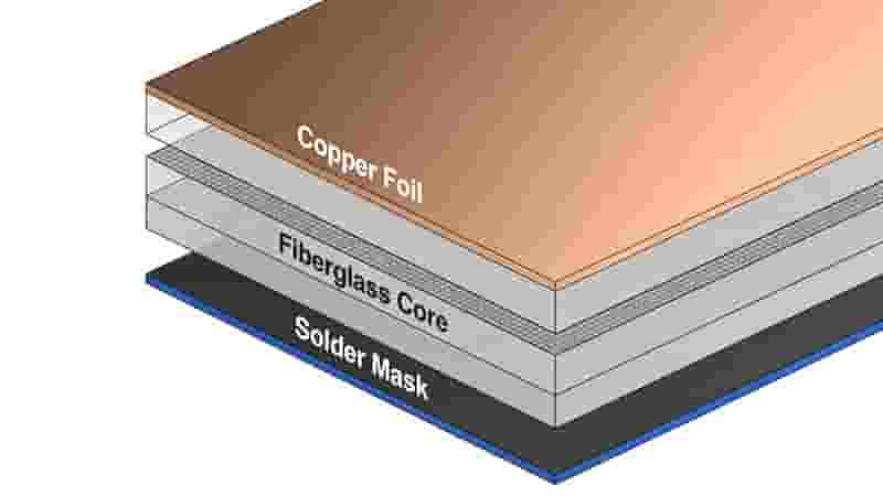
HASL (Hot Air Solder Leveling) is a mature, industrial‑grade PCB surface finish that coats exposed copper circuits with a layer of molten solder. The process uses high‑temperature air knives to create a uniform, protective layer that prevents oxidation and ensures strong solder joints during assembly.
For decades, HASL has been the industry standard for its balance of cost, reliability, and compatibility with most assembly processes. We provide both traditional and lead‑free HASL to meet global regulatory requirements such as RoHS and REACH.
How the HASL Process Works
The HASL process follows a strict, repeatable flow to ensure consistent quality for mass production:
- Pre‑cleaning to remove oils, oxides, and contaminants
- Preheating to avoid thermal shock to the PCB substrate
- Flux application to improve solder wetting
- Immersion in molten solder alloy
- Hot air knife leveling for uniform coating thickness
- Post‑cleaning and inspection
Key Benefits of HASL PCB Surface Finish
HASL remains a top choice for global buyers and engineers due to these advantages:
- Lowest cost among common PCB surface finish options
- Excellent solderability for through‑hole and standard SMT components
- Strong oxidation resistance for long‑term storage
- Easy rework and repair during assembly
- Proven reliability in high‑volume production
- Compatible with most PCB base materials
Limitations of HASL
While HASL performs well for most applications, it has constraints for advanced designs:
- Uneven coating thickness, not ideal for fine‑pitch SMT
- Higher thermal exposure during processing
- Less suitable for ultra‑thin or high‑frequency PCBs
- May cause minor bridging in small plated‑through holes
Lead‑Free HASL vs Traditional HASL
We offer both versions to match your project’s regulatory and performance needs:
| Item | Traditional HASL | Lead‑Free HASL |
|---|---|---|
| Alloy | Sn63/Pb37 | SnCuNi (RoHS) |
| Melting Point | Lower | Higher |
| Regulatory | Non‑RoHS | RoHS & REACH |
| Cost | Lower | Slightly higher |
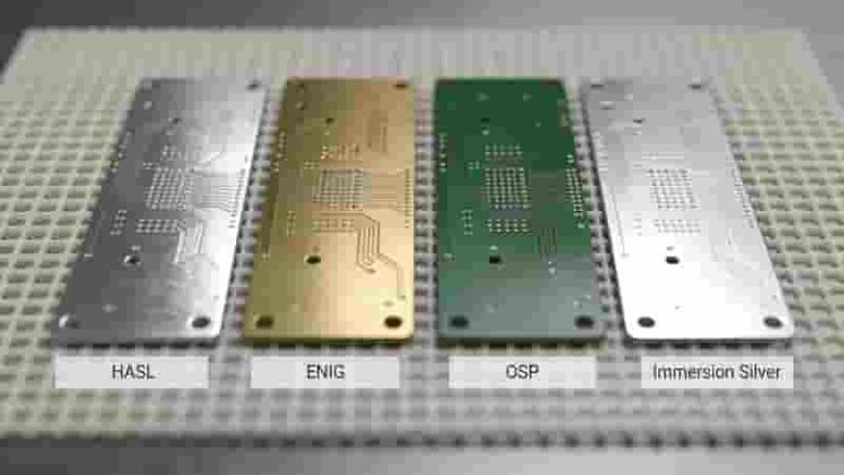
HASL vs Other PCB Surface Finishes
Conclusion
HASL is a time‑tested, cost‑effective PCB surface finish that delivers consistent performance for most electronic devices. It balances affordability, solderability, and durability better than many alternatives. For standard to mid‑range PCB projects, HASL remains the most practical choice for global buyers.
We provide full‑process HASL and lead‑free HASL services with strict quality control, fast lead times, and competitive pricing for international importers, engineers, and contract manufacturers.
Get Your HASL PCB Quote Today
Contact us for free DFM check, custom manufacturing, and competitive pricing for your PCB project.
Request a Quote
What Is Prototype PCB Assembly
Aluminum PCB vs FR4 PCB: Full Technical Comparison for Industrial & Export Buyers
Surface Mount Technology (SMT): Advantages, Limitations & Applications
SMT PCB Assembly Services for Prototypes & Production
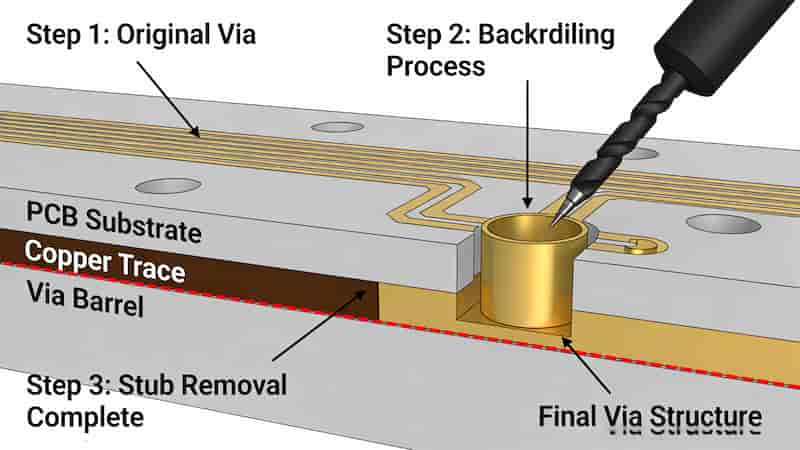
Backdrilling of Vias: The Definitive Guide for High-Speed PCB Signal Integrity