PCB Materials Surface Finishes Prototype Manufacturing Canada

Fast Prototype PCB Manufacturing Services in Canada 

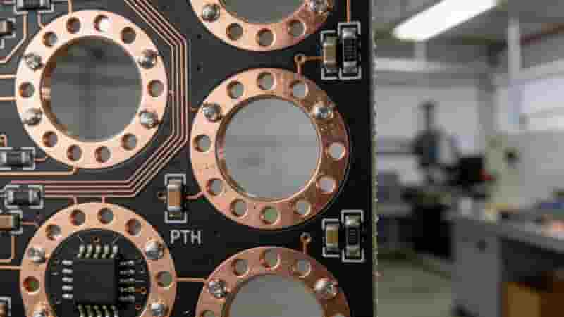
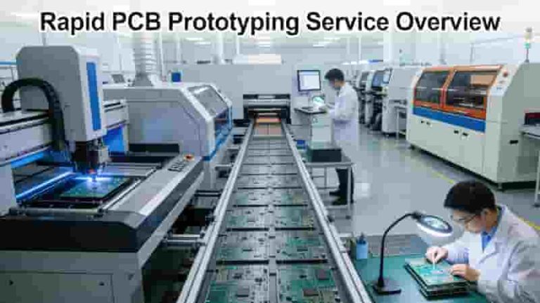
Fast Prototype PCB Manufacturing Services in Canada provide rapid, high‑reliability printed circuit board prototyping for engineers, procurement teams, and OEMs across Canada. We offer quick‑turn rigid, flexible, rigid‑flex, HDI, and high‑frequency PCBs with IPC Class 2/3 standards, DFM support, 48–72 hour lead times, and seamless scaling to volume production.

Core Prototyping Capabilities

Our fast prototype PCB manufacturing supports full‑range specifications to meet Canadian product development demands.

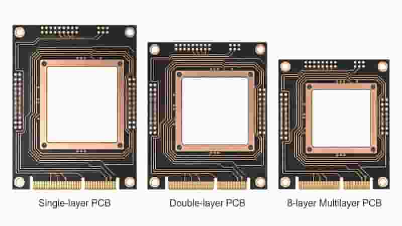
  • Layer count: 1–64 layers (single‑sided, double‑sided, multilayer, HDI)
  • Board thickness: 0.4mm–3.2mm
  • Max size: 24×24 inches
  • Minimum order: 5 pieces
  • Lead time: 48–72 hours for standard designs
  • Full electrical testing & AOI inspection
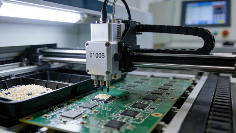
  • Optional SMT assembly & turnkey solutions
PCB Prototype Capabilities Canada Fast Prototype Manufacturing

Materials & Surface Finishes

We use certified materials for prototype PCB manufacturing compatible with industrial, automotive, and IoT applications in Canada.

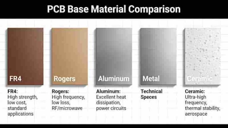
  • Base materials: FR‑4, High‑Tg FR‑4, Rogers, PTFE, aluminum, copper core
  • Surface finishes: HASL, lead‑free HASL, immersion gold, ENIG, immersion silver, immersion tin
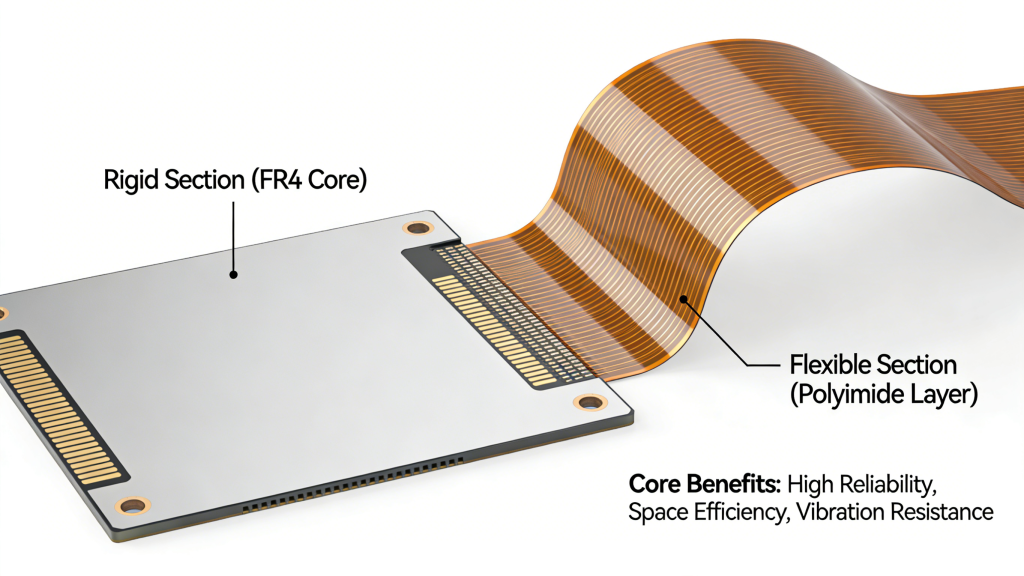
  • Special types: flexible PCB, rigid‑flex PCB, metal core PCB, high‑frequency PCB
PCB Materials Surface Finishes Prototype Manufacturing Canada

Quality & Industry Standards

Our fast prototype PCB services follow strict international standards to ensure reliability for Canadian clients.

  • ISO 9001 & IATF 16949 certified
  • IPC‑A‑600 Class 2 / Class 3 compliance
  • 100% electrical test before shipment
  • Full DFM analysis free of charge
  • RoHS & REACH compliant materials

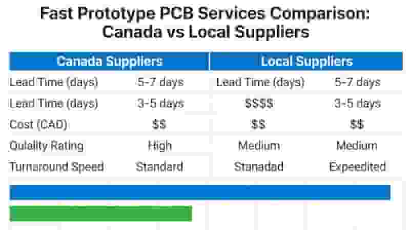
Advantages for Canadian Customers

We deliver better value for prototype PCB in Canada compared to local suppliers.

ItemOur ServicesLocal Canadian Suppliers
Lead Time48–72 hours7–10+ days
Cost50–60% lowerHigher
Material OptionsFull rangeLimited
DFM SupportFreePaid or limited
  • Speed: Accelerate product development cycles
  • Cost: Lower prototype expenses without losing quality
  • Flexibility: Wide material and customization choices
  • Scalability: Smoothly move from prototype to mass production
  • Shipping: Reliable delivery via DHL / FedEx to Canada in 3–5 days
Fast Prototype PCB Advantages Canada Compared to Local

Design & Ordering Guide

Streamline your fast prototype PCB manufacturing process with our simple workflow.

  1. Prepare Gerber files, BOM, and stackup requirements
  2. Submit files for a free DFM check and instant quote
  3. Confirm design and place order
  4. Manufacturing and full testing (48–72 hours)
  5. Express shipping to your address in Canada
Fast Prototype PCB Order Process Canada Workflow

Frequently Asked Questions

Q: How fast can you deliver prototype PCBs to Canada?
A: Standard fast prototype PCB manufacturing lead time is 48–72 hours, plus 3–5 days shipping to Canada.

Q: What is the minimum order quantity?
A: We accept orders starting from 5 pieces for prototype PCB in Canada.

Q: Do you provide free DFM analysis?
A: Yes, we offer free DFM checks to optimize your design for prototype PCB manufacturing.

Q: Can you handle flexible and rigid‑flex PCBs?
A: Yes, we support flexible, rigid‑flex, HDI, and high‑frequency prototypes for Canadian clients.

Conclusion

Our fast prototype PCB manufacturing services in Canada combine speed, quality, and cost efficiency to support product developers across industries. With short lead times, international certifications, full material options, and professional engineering support, we are a trusted partner for your PCB prototyping needs.

Get Your Fast PCB Prototype Quote Today

Send your Gerber files for a free quote and DFM analysis. We support fast prototype PCB manufacturing for all Canadian projects.

Request a Quote

PCB Copper Electroplating Machine for Fast Production

Rapid PCB Prototyping and Production: Accelerate Your Product Launch

In today’s fast‑paced product development cycles, rapid PCB prototyping and accelerated production services are critical for first‑mover advantage. This guide covers quick‑turn turnaround times, fast PCB manufacturing lead times, and how express PCB solutions support agile hardware design and faster time‑to‑market. Why Rapid PCB Prototyping and Production Matter In today’s fast‑paced product development world, time…
PCB basic structure diagram showing trace pad silkscreen component

PCB Terminology Glossary – Over 150 Essential PCB Terms for Engineers & Global Buyers

This professional PCB glossary provides clear, industry-standard definitions for over 150 key terms used in PCB design, manufacturing, assembly, and quality control. Ideal for engineers, procurement teams, and global buyers, this resource helps streamline communication, avoid misunderstandings, and ensure accurate project execution. We continuously update this list to cover the latest technologies and standards in…
Professional PCBA Manufacturing Line SMT Production

Printed Circuit Board Assembly Services | Full Turnkey PCBA Solutions

Printed Circuit Board Assembly Services provide professional SMT, through-hole, BGA, and mixed-technology assembly for global electronics buyers. We support prototype to mass production, strict quality control, fast turnaround, and cost-effective one-stop EMS solutions for industrial, automotive, medical, and communication applications. PCBA Expert & Professional Manufacturer We are a professional Printed Circuit Board Assembly Services provider…

PCB Stackup Design Guidelines: Best Practices for 2, 4, 6 Layers

PCB stackup design directly determines signal integrity, EMI control, power stability and manufacturing reliability. This guideline provides professional, field-proven best practices for 2‑layer PCB stackup, 4‑layer PCB stackup and 6‑layer PCB stackup for industrial electronics, communications equipment and high‑speed digital products. Introduction to PCB Stackup Design PCB stackup design is the foundation of high‑performance printed…
FR-4 PCB material structure fiberglass epoxy laminate

Why Choose FR-4 PCBs in 2025? Benefits, Applications & Custom Solutions for 5G, IoT & EVs

FR-4 PCBs remain the global industry standard in 2025, delivering unmatched cost‑efficiency, reliability, and versatility for 5G, IoT, electric vehicle, and industrial electronics. This guide explains core properties, advantages, material comparisons, and why FR‑4 is still the top choice for engineers and global buyers. Introduction: Dominance of FR-4 in PCB Manufacturing Printed circuit boards are…
FR-4

PCB Materials Classification & Substrate Selection Guide

Today, almost all electronic devices use PCBs (Printed Circuit Boards)—from satellites to wristwatches. PCBs have 3 key benefits: Here’s the critical part: Your project’s performance depends on your PCB material. Cheap PCBs often fail to deliver accurate results. To avoid project risks, follow 3 simple steps: 1. What is PCB Material? A PCB (Printed Circuit…

Similar Posts