|

Accelerate Your Innovation with Rapid PCB Prototyping

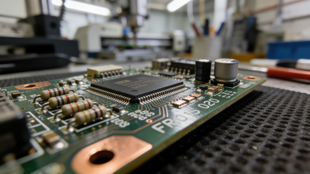
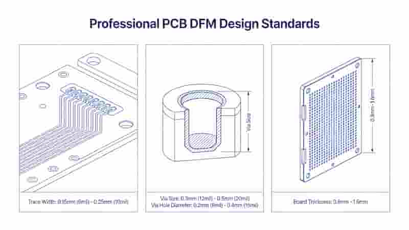
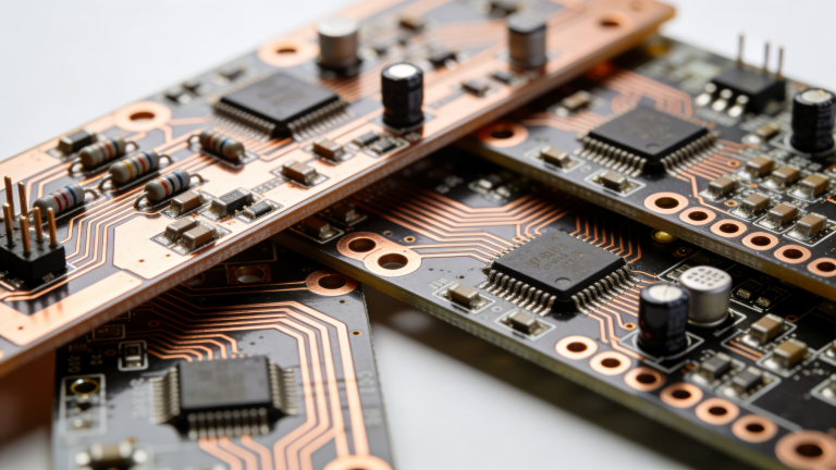
PCB prototyping process for design validation and testing

We provide professional Rapid PCB Prototyping with ultra‑fast lead times, strict quality control, and full customization for global engineers and buyers. From prototype to small‑batch production, we speed up your innovation and time‑to‑market.
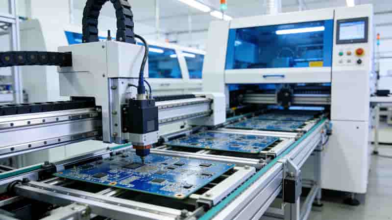
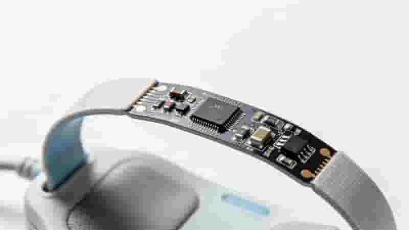
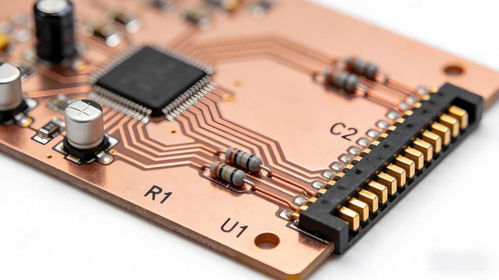
Rapid PCB Prototyping for fast product development and engineering validation

What Is Rapid PCB Prototyping

Rapid PCB Prototyping is the fast production of small‑batch printed circuit boards to validate design, function, and reliability before mass production. It helps engineers detect flaws early, optimize performance, and shorten product development cycles dramatically.

Our rapid PCB prototyping supports single‑sided, double‑sided, multilayer, rigid, flexible, and rigid‑flex boards to match modern electronic product demands.
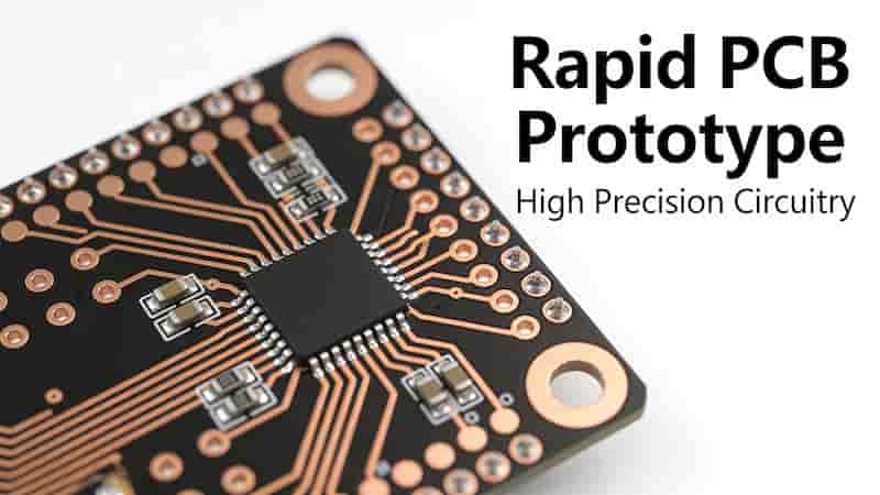
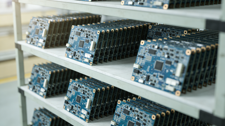
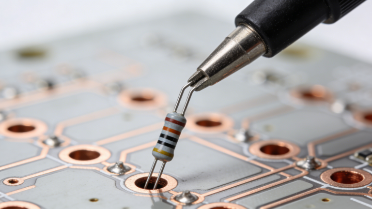
PCB prototyping process for design validation and testing

Why Choose Us for Rapid PCB Prototyping

We focus on speed, quality, and stability to support your innovation. Our advantages make us a reliable partner for global buyers:

  • Ultra‑fast turnaround: 8 hours for double‑sided prototypes, 24–72 hours for multilayer
  • Strict quality: IPC Class 2, RoHS, UL certified production
  • Low MOQ: 5–100 pieces for prototype testing and iteration
  • Full services: PCB fabrication + SMT assembly + component sourcing
  • Free DFM review to optimize design and avoid production risks
  • Global delivery: DHL, FedEx, UPS for fast and safe shipping
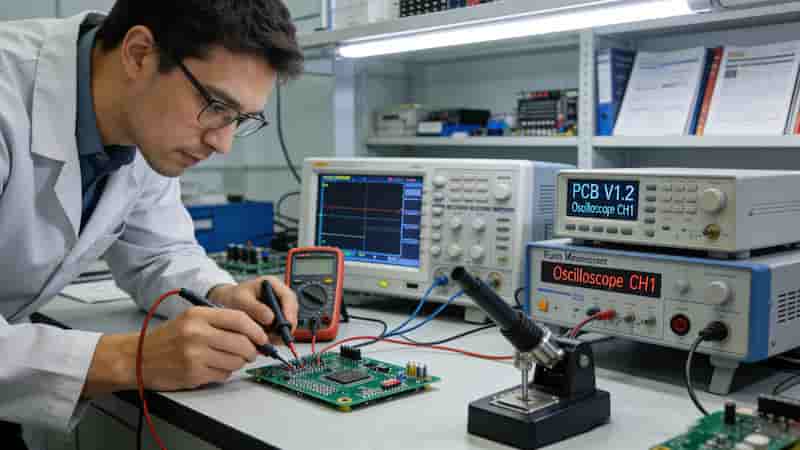
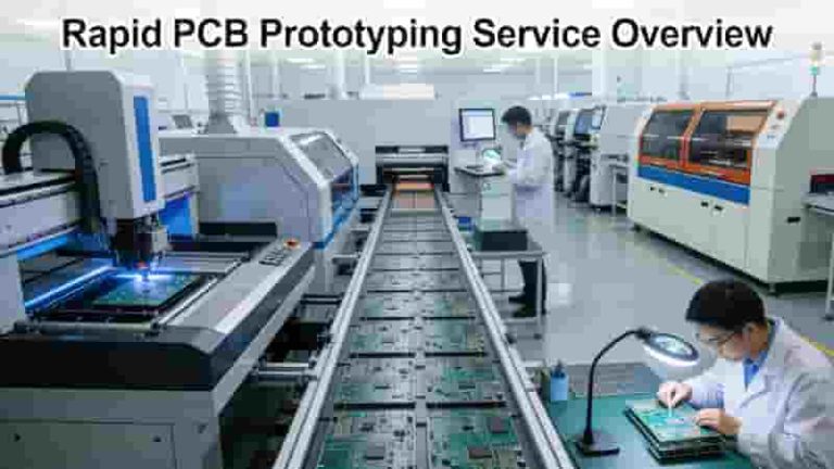
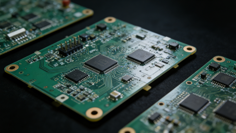
Professional rapid PCB prototyping manufacturing line

Key Benefits of Fast-Turn PCB Prototyping

Speed Up Time-to-Market
Fast rapid PCB prototyping cuts development cycles, helping you launch products ahead of competitors.

Ensure Stable & Reliable Design
Test and adjust early to eliminate hidden risks before mass production.

Reduce Overall Cost
Avoid expensive rework by validating designs in the prototype stage.

Support Complex Customization
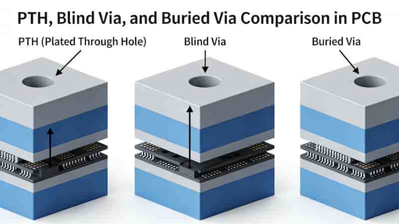
We handle multilayer PCBs, blind vias, buried vias, flexible and rigid‑flex structures.

Rapid PCB Prototyping Lead Time Table

LayersWithin 0.1㎡0.1–1㎡1–2㎡
Single-layer24h / 48h24h / 48h3d / 5d
Double-layer8h / 24h24h / 48h3d / 7d
4 Layer2d / 3d3d / 4d4d / 8d
6 Layer3d / 4d4d / 5d5d / 10d
8 Layer3d / 4d4d / 5d6d / 11d

How to Get Rapid PCB Prototypes

1. Prepare your Gerber files and production requirements

2. Send files to get a free, fast quote

3. Confirm design and start rapid PCB prototyping

4. Full quality inspection before delivery

5. Fast global shipping to your address

Summary

Rapid PCB Prototyping is essential for modern product innovation. We deliver fast turnaround, high quality, full customization, and professional support to help engineers and buyers accelerate development, reduce risks, and launch products faster.

Start Your Rapid PCB Prototyping Now

Get free DFM check, fast quote, and high-quality rapid PCB prototyping in 8–72 hours.

Request a Free Quote
Contact for rapid PCB prototyping quote and custom service
Plated Through Hole PTH Structure in PCB

What is the Difference Between PTH and Via in PCBs?

Posted on
0 Comments
Understanding the key differences between PTH and via is essential for optimizing PCB design and manufacturing. This article defines PTH and via, compares dimensions, functions, locations and finishing requirements. Typical applications and design considerations are also discussed. Defining PTH and Vias in PCBs PCBs serve as the foundation for almost all modern electronics. They provide…
Rogers PCB material types RO4000 RO3000 RT duroid laminate series

Rogers PCB: Full Guide to High-Frequency & High-Speed Circuit Boards

Posted on
0 Comments
Rogers PCB is the leading solution for high‑frequency electronics. This guide covers properties, types, benefits, applications, and comparisons between Rogers PCB, FR‑4, and Teflon PCBs, ideal for engineers and manufacturers looking for advanced circuit solutions. What is Rogers PCB? Rogers PCB refers to printed circuit boards using advanced laminate materials produced by Rogers Corporation. Unlike…
PCB Manufacturer in South Africa - Professional PCB Production Line

PCB Manufacturer in South Africa | Reliable Custom PCB & PCBA Services 

Posted on
0 Comments
Looking for a trusted PCB manufacturer in South Africa for prototypes, mass production, or full PCBA? We deliver high-quality, cost-effective PCB manufacturing and assembly solutions to industrial buyers, engineers, and procurement teams across South Africa.  Local PCB Manufacturing in South Africa  We are a professional local PCB manufacturer serving South Africa with flexible lead times…
Metal Core PCB cross section structure aluminum copper thermal dielectric layer

Metal Core PCB (MCPCB) Manufacturing Service in China

Posted on
0 Comments
We are a professional Metal Core PCB manufacturer in China, providing fast MCPCB prototypes and small-batch production with aluminum and copper cores at competitive prices for LED and power electronics. Why Metal Core PCBs (MCPCBs) for High-Power Designs High-power electronic designs face critical thermal management challenges that traditional FR4 PCBs cannot adequately address. Metal Core…
RoHS restricted substances limits for PCB materials and assembly

RoHS Compliant PCBs: Complete Guide to Standards, Manufacturing & Testing 

Posted on
0 Comments
RoHS Compliant PCBs are essential for global market access. This guide covers restricted substances, compliance benefits, lead-free processes, assembly, testing, and how to partner with trusted RoHS compliant PCB manufacturers. Introduction to RoHS Standards RoHS (Restriction of Hazardous Substances) is an EU directive that limits hazardous materials in electrical and electronic products. For printed circuit…
Multilayer PCB stackup basics core prepreg copper layers structure

Multilayer PCB Layer Stackup And Thickness Guide: Standard 4‑Layer to 14‑Layer Configurations

Posted on
0 Comments
Multilayer PCB stackup and thickness directly determine signal integrity, EMC performance, mechanical stability and manufacturability. This professional guide covers core principles, key parameters, standard stackups from 4‑layer to 14‑layer, thickness selection and engineering best practices for industrial electronics, high‑speed designs and critical applications. Why Multilayer PCB Stackup And Thickness Matter Modern electronics demand smaller size,…

FAQs About Rapid PCB Prototyping Service

A: Double-sided PCBs can be finished in 8 hours. Multilayer prototypes take 24 to 72 hours based on layer count and board size.

A: We support single-sided, double-sided, multilayer, rigid, flexible and rigid-flex PCBs, including designs with blind and buried vias.

A: MOQ starts from 5 pieces, suitable for prototype verification and multiple design iterations.

A: All products follow IPC Class 2, RoHS and UL requirements with complete quality control.

A: Yes. We provide PCB fabrication, component sourcing, SMT assembly and complimentary DFM review.

A: Please submit Gerber files and detailed production requirements to get a prompt quotation.

A: We use DHL, FedEx and UPS to deliver orders worldwide quickly and safely.

A: It shortens development cycles, removes potential risks, cuts post-production rework costs and supports complex customized designs.

Similar Posts