Complete professional guide to multilayer PCB stackup design, standard thicknesses, layer arrangements, impedance control, and ready-to-use 4–14 layer configurations for industrial, high-speed, and high-reliability electronics.
Why Multilayer PCB Stackup and Thickness Matter
Today’s electronics demand smaller size, higher speed, greater integration, and longer reliability. Multilayer PCB stackup and total board thickness directly determine signal integrity, EMC/EMI performance, impedance control, thermal management, and mechanical stability.
A well-designed stackup supports controlled impedance, reduces crosstalk, stabilizes power delivery, and minimizes warpage. Poor stackup design leads to signal reflection, noise, EMI failures, and reliability risks—even with correct schematics and layout.
This guide explains professional PCB stackup principles, thickness drivers, and industry-standard 4–14 layer setups used globally by engineers and manufacturers.
PCB Stackup Basics: Core, Prepreg and Copper Layers
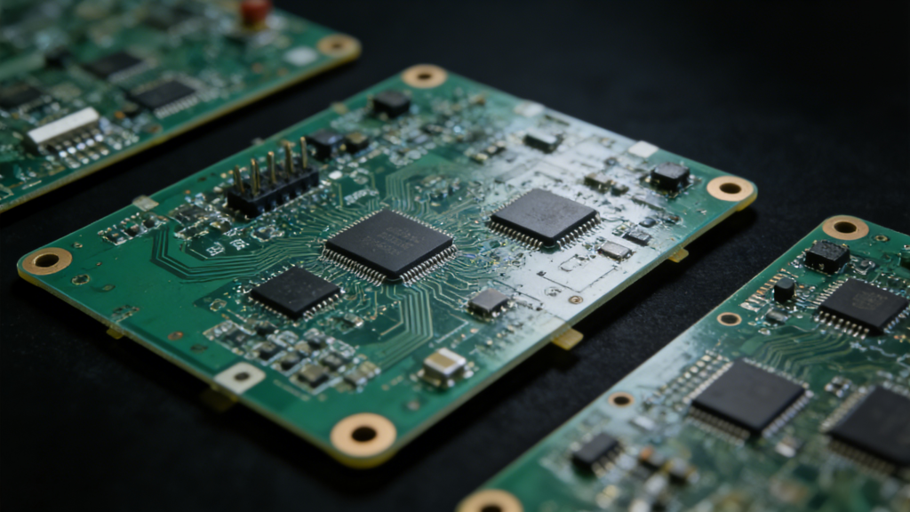
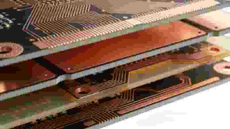
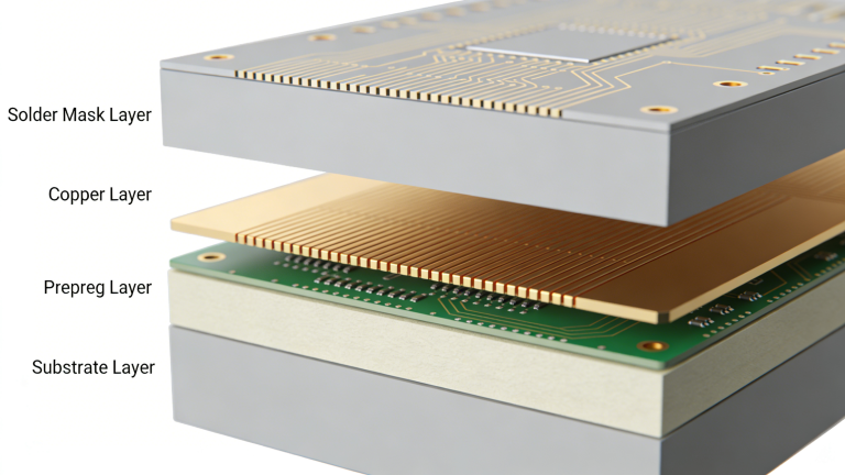
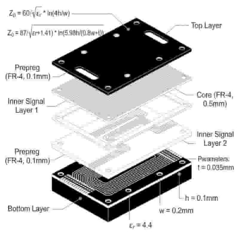
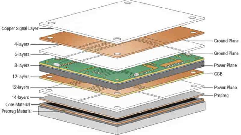
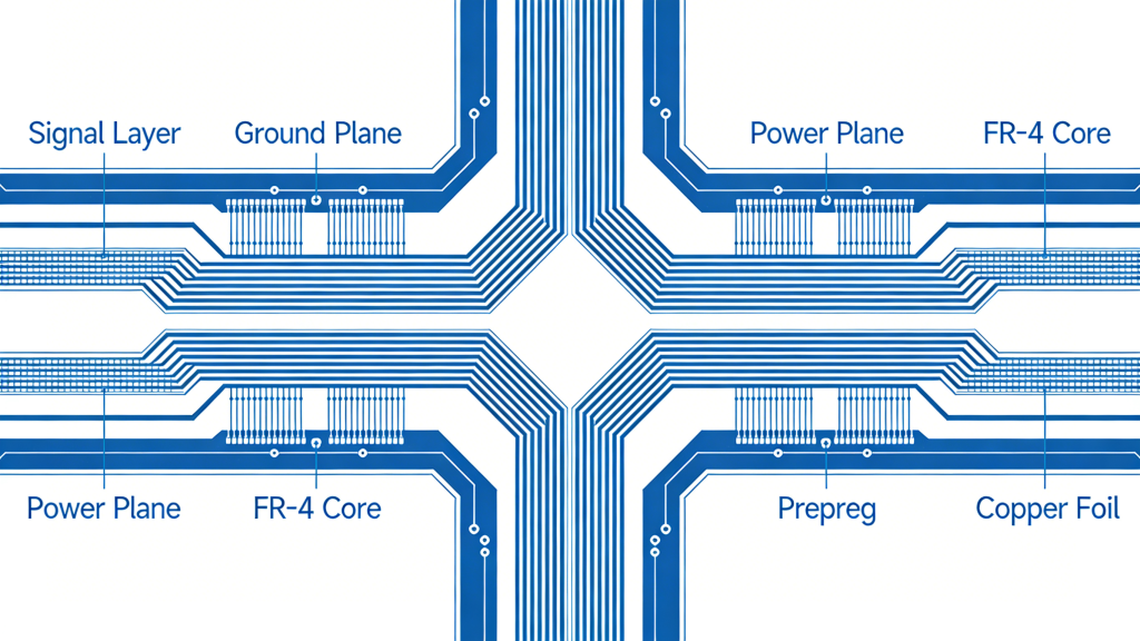
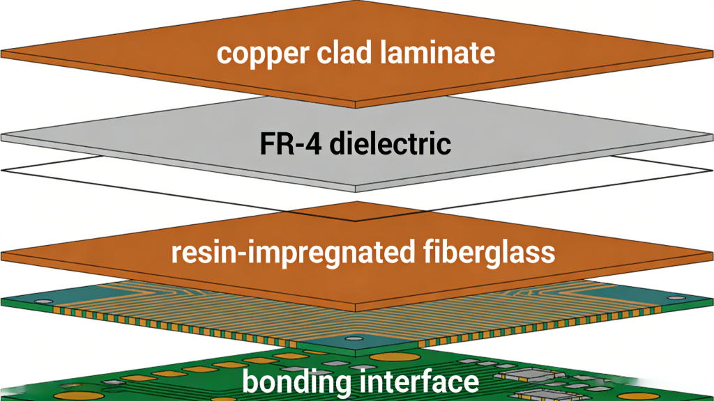
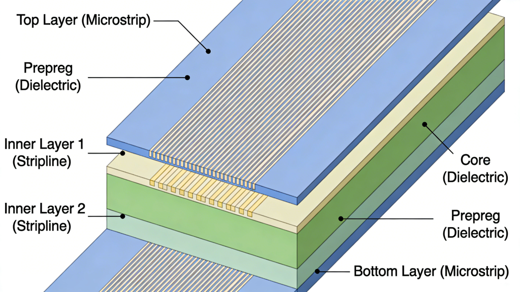
A multilayer PCB stackup is the engineered arrangement of signal layers, ground planes, power planes, core substrates, and prepreg materials. Symmetrical design prevents warpage and simplifies manufacturing.
- Core: Rigid copper-clamped dielectric (FR‑4 standard) that forms the board structure.
- Prepreg: Resin‑impregnated fiberglass used to bond layers during lamination.
- Copper Foils: Provide conductive paths; standard 1 oz, 2 oz for high-current designs.
Balanced stackups mirror layers around the center axis, ensuring consistent stress distribution and impedance stability.
Key Factors That Affect Multilayer PCB Thickness
Final thickness depends on electrical, mechanical, and manufacturing requirements:
- Layer count and plane/signal arrangement
- Core and prepreg thickness selection
- Copper weight (1 oz, 2 oz, 3 oz)
- Impedance control requirements (50Ω, 75Ω, 90Ω, 100Ω differential)
- Mechanical strength, connector compatibility, and enclosure limits
- Thermal performance and reliability needs
- Manufacturing capabilities and cost efficiency
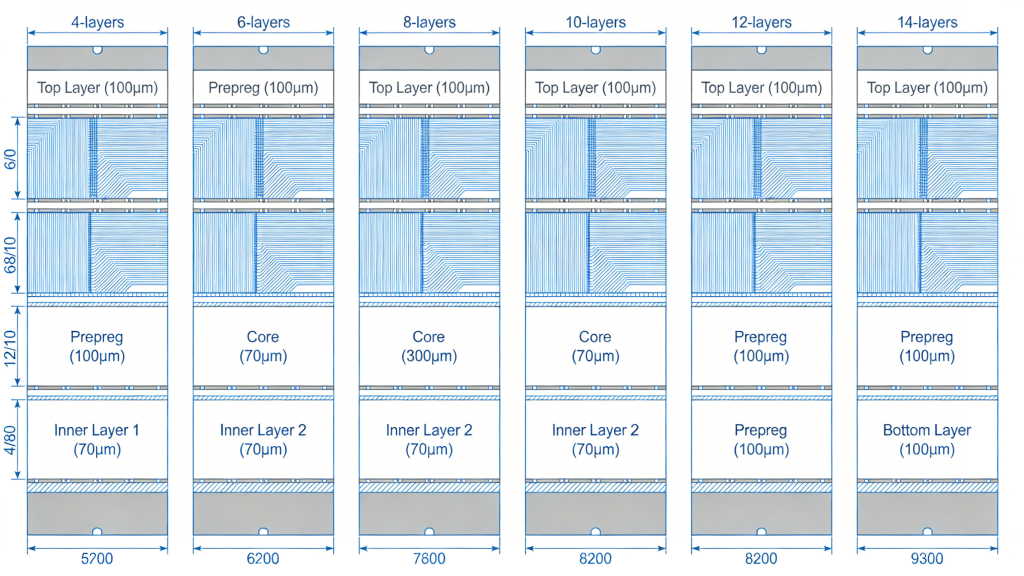
Standard 4–14 Layer PCB Stackup and Thickness Options
4-Layer PCB Stackup (Most Common)
Standard thickness: 1.6 mm; range: 1.0–2.4 mm
Typical layer order:
- L1: Top Signal
- L2: GND Plane
- L3: PWR Plane
- L4: Bottom Signal
Ideal for industrial controls, IoT, consumer electronics, and general-purpose circuits.
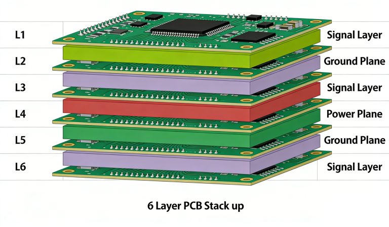
6-Layer PCB Stackup
Standard thickness: 1.6–2.0 mm
Supports high-speed signals, improved EMI shielding, and mixed-signal separation.
8/10/12/14-Layer PCB Stackup
Standard thickness: 2.0–3.0 mm
Designed for high-speed networking, servers, FPGA/SoC, telecom, medical, and aerospace systems with strict signal integrity demands.
Multilayer PCB Stackup Comparison Table
| Layer Count | Standard Thickness | Best For |
|---|---|---|
| 4 Layer | 1.6 mm | IoT, Industrial Controls |
| 6 Layer | 1.6–2.0 mm | High-Speed, Mixed-Signal |
| 8–12 Layer | 2.0–2.4 mm | Telecom, FPGA, Networking |
| 14 Layer | 2.4–3.0 mm | High-End Computing, 5G, Aerospace |
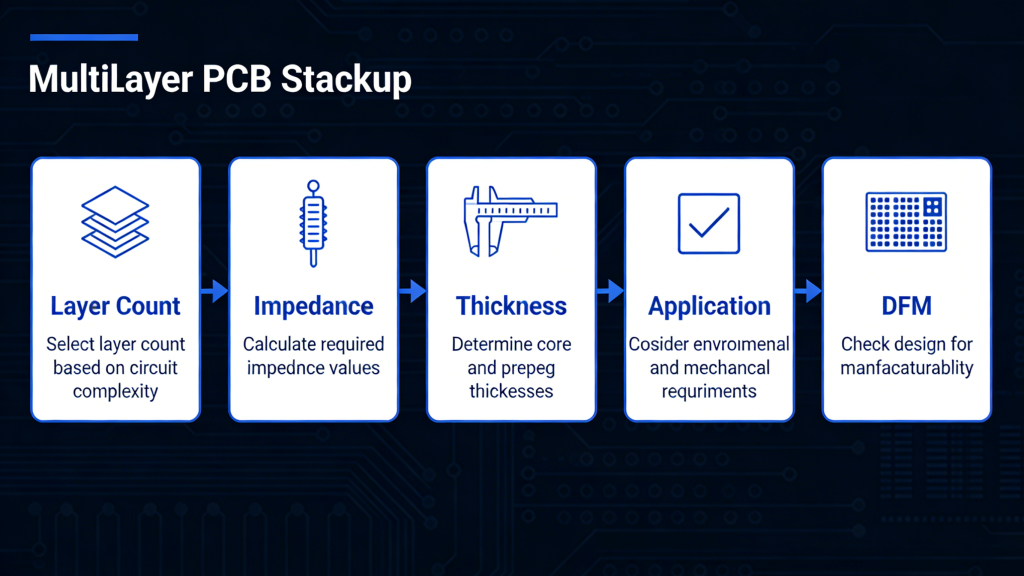
How to Choose the Right Multilayer PCB Stackup
- Define signal speed, impedance, power domains, and mechanical constraints
- Select layer count based on routing density and EMC needs
- Choose industry-standard thickness for cost and reliability
- Use symmetrical stackup to avoid warpage
- Confirm impedance and DFM with our engineering team
Conclusion
Multilayer PCB stackup and thickness are foundational to performance, yield, and cost. Standard 4–14 layer configurations provide proven solutions for high-speed, industrial, and mission-critical applications.
By following symmetrical design, controlled impedance, and standard thickness rules, you ensure reliable manufacturing and stable electrical performance.
Get Your Custom Multilayer PCB Solution
Need optimized PCB stackup design, free DFM review, or precise quotation for 4–14 layer boards? Our engineering team supports your project from concept to mass production.
Request Free Quote
Contact Engineering Team
High Volume PCB Assembly Services
Aluminum PCB Manufacturing Process: Step-by-Step Guide
Impedance Control PCB Fabrication Services
Double-sided PCB Manufacturing Process – We Deliver Compliant, Efficient Production

High-Performance Copper Core PCBs for LED and Power Applications