Double-sided PCB is the most widely used and preferred type of PCB in the industry. Its advantage lies in the balanced positioning — it avoids the high complexity of multilayer PCBs while overcoming the functional limitations of single-layer PCBs, making it a cost-effective choice for most electronic projects.
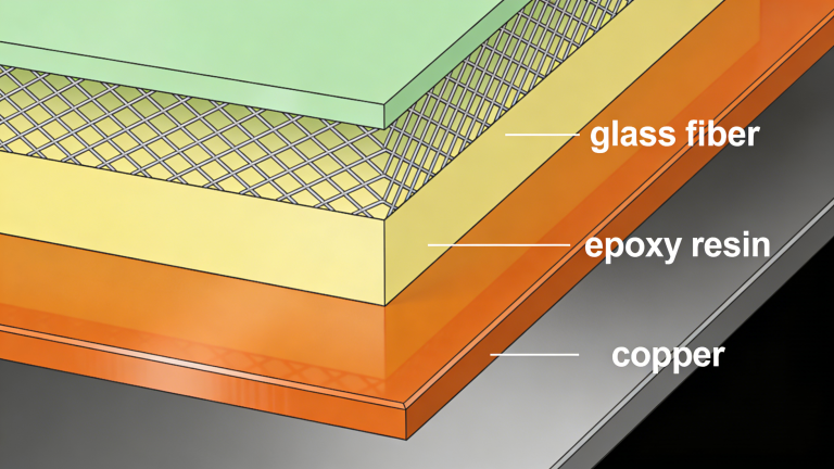
Unlike single-layer PCBs that only support component mounting on one side, double-sided PCBs feature two conductive layers (one on each side of the substrate). The stack-up structure is relatively simple, with no need for inner layers — this not only simplifies the manufacturing process but also significantly improves space utilization.
By allowing components to be placed on both sides, double-sided PCBs achieve a more compact design. This is particularly valuable for electronic devices that require miniaturization (such as consumer electronics and industrial control equipment), as it reduces the overall size of the circuit board without compromising functional density.
Common types of double-sided PCB manufacturing processes include:
- Double Sided PCB Fabrication Process
- Double Layer PCB Manufacturing Process (with flow chart)
- Double-Layer PCB Manufacturing Process for HASL-LF / Immersion Gold Surface Finish
- Double-sided PCB with Gold Plating Manufacturing Process (with flow chart)
Click here to Download the Double-sided PCB Manufacturing Process PPT
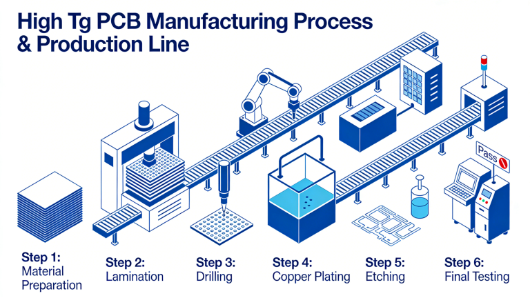
PCB manufacturing is a systematic process that transforms raw materials into functional double-sided PCBs through multiple controlled steps. Below is a detailed, step-by-step explanation of the complete manufacturing process, covering both technical details and practical significance.
Pre-Manufacturing Preparation (3 Steps)
Step 1: PCB Circuit Design
The first step is to create a schematic diagram, which serves as the blueprint for the circuit. We offer more than 30 free PCB design software options for download. Based on industry practice, EDA and Eagle are recommended for their stability and compatibility with manufacturing requirements.
Step 2: PCB Layout Design
After finalizing the schematic, start the layout design (Eagle EDA is commonly used). The layout is then printed on glossy paper using a laser printer.
⚠️ Critical Note: Before printing the top layer layout, mirror the image—failure to do so will result in an inverted circuit, rendering the PCB unusable.
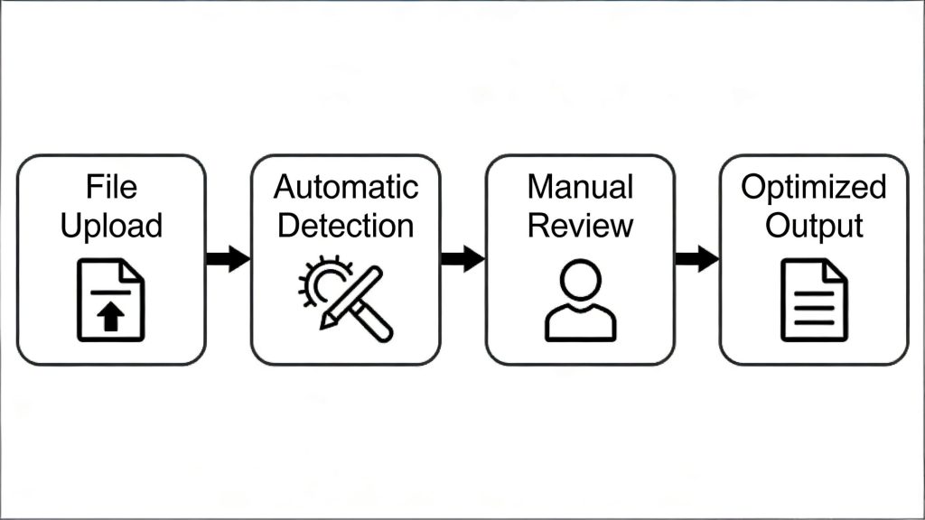
Step 3: DFM Check (Design for Manufacturability)
This step verifies if the customer-provided design files align with actual manufacturing capabilities. Engineers often focus on functional design but may overlook manufacturing limitations (e.g., trace width, hole size).
- Our experts inspect traces, layers, holes, and pads to fix flaws (e.g., overly narrow traces, non-standard hole diameters).
- Only after passing DFM check are the files sent to the production line—this avoids delays and material waste caused by unmanufacturable designs.
Core Manufacturing Process (13 Steps)
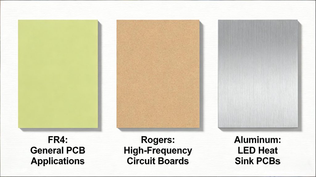
Step 4: Selection of PCB Materials
Choose substrates based on application requirements—different materials offer distinct performance and cost advantages:
- FR4: The most widely used flame-retardant substrate. Economical, affordable, and maintains stability under extreme temperatures (suitable for most general electronic products).
- High-frequency materials (e.g., Rogers RO4000 series, Taconic TLX series): Used for high-frequency/high-speed PCBs (FR4 cannot meet signal transmission requirements in such scenarios).
- Metal substrates (aluminum, copper, iron): Applied to LED PCBs in the lighting industry (excellent heat dissipation).
Note: Copper-clad laminate (CCL) is the core raw material for PCBs—our factory stores CCL in a controlled environment to prevent moisture absorption and oxidation.
Step 5: Cutting of CCL (Copper Clad Laminate)
Raw CCL comes in large standard sizes (e.g., 37×49 inches, 41×49 inches, 43×49 inches) and needs to be cut into production-friendly sizes:
- The cut size is larger than the final PCB size—multiple PCBs (even from different customers) are arranged on one panel to maximize material utilization and reduce costs. Example: For 5 pieces of 4×4 inch PCBs, we arrange them on a larger panel with other small PCBs, then separate them after manufacturing.
- After cutting, the panel edges are smoothed and trimmed to avoid burrs that could damage equipment in subsequent steps.
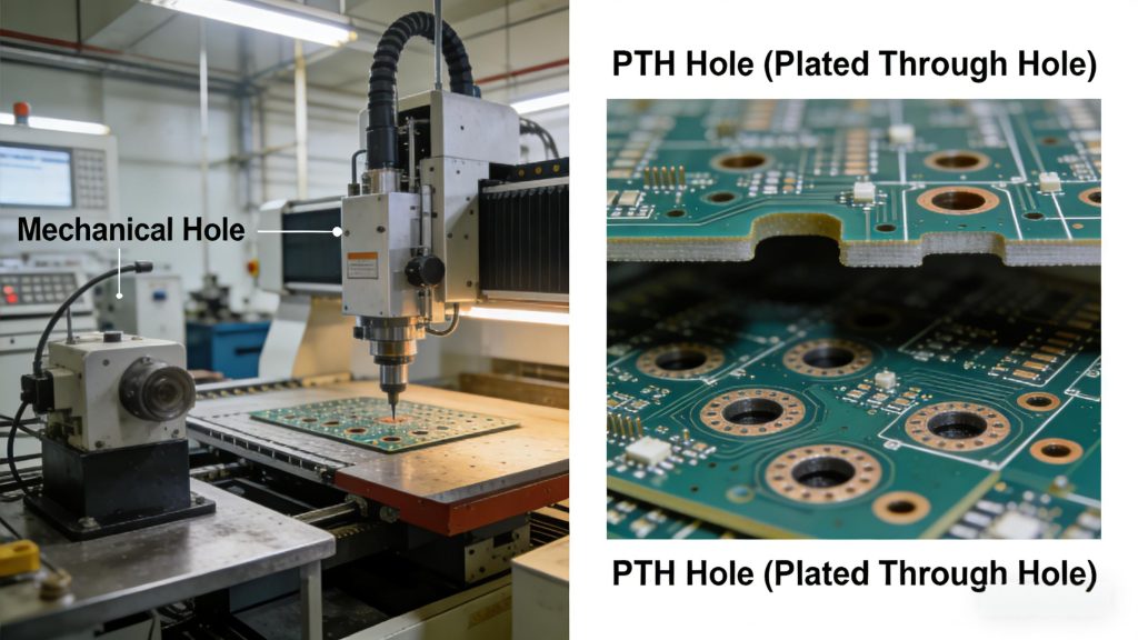
Step 6: Drilling
Panels are sent to automatic drilling machines (equipped with auto drill bit changing) for precise hole creation. There are two main types of holes:
- Mechanical holes: Located at panel edges, used for fixing the PCB with screws.
- Vias: Critical for circuit connectivity (only Plated Through Holes (PTH) are used for double-sided PCBs—blind/buried vias are for multilayer PCBs):
- PTH penetrates the entire panel, connecting components on both sides (no inner layers in double-sided PCBs, so no need for other via types).
- After drilling, panels are cleaned in a chamber to remove debris, then the hole walls are prepped for copper plating.
Step 7: Electroless Copper Deposition (Plating Through Holes)
Hole walls are initially made of epoxy (non-conductive)—electroless copper deposition is required to create conductivity:
- The panel is dipped in electroless copper solution to form a thin copper layer on hole walls.
- Subsequent acid dipping and anti-tarnish treatment prevent oxidation.
- Two process types: Horizontal (for carbon deposition, prepping hole walls) and Vertical (for copper deposition, ensuring conductivity).
Key Role: This step is essential for double-sided/multilayer PCBs—it enables electrical connection between the two conductive layers.
Step 8: Photo Imaging and Printing of Circuit
This step transfers the circuit pattern onto the panel using photolithography:
- A photoresistive film (sensitive to UV light) is hot-rolled onto the panel (both sides).
- The operation is done in a yellow-light room—other light wavelengths would prematurely harden the photoresist.
- A film with the circuit pattern is placed over the panel, then passed through a UV light chamber:
- UV light hardens the photoresist in areas corresponding to the circuit.
- Unhardened photoresist (non-circuit areas) remains soft for subsequent removal.
Step 9: Pattern Plating
Plating ensures the copper layer meets thickness requirements (specified by customers):
- The panel is cleaned and activated in chemical baths, then electroplated (computer-controlled to ensure precise bath time).
- Copper plating: IPC 600J-Class 2 standard requires a minimum 18μm copper layer on hole walls (we typically plate 20μm for reliability). Surface traces also get a 20μm copper layer.
- Tin plating: A thin tin layer is plated over copper—this acts as a protective mask during etching (prevents desired copper from being removed).
Technical Note: Modern plating baths have excellent “throwing power,” ensuring uniform copper thickness across the panel and inside holes.
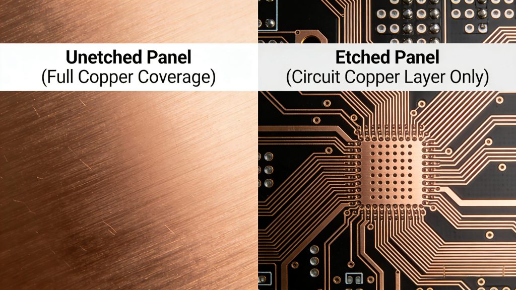
Step 10: Developing and Etching
These two steps remove excess copper and leave only the desired circuit:
- Developing: The panel is dipped in a developing solution to remove unhardened photoresist (exposing excess copper).
- Etching: The panel is immersed in an etching solution—this dissolves the exposed excess copper. The tin-plated (hardened photoresist) areas remain intact.
- Post-etching cleaning: The remaining tin layer and hardened photoresist are removed via washing, leaving a clear circuit pattern on both sides of the panel.
Step 11: Automatic Optical Inspection (AOI)
AOI detects defects after etching (e.g., open circuits, short circuits, missing traces) using high-resolution cameras:
- Cameras capture images from multiple angles, then compare them with the original design file.
- Defective panels are automatically separated from the production line (process takes only a few seconds per panel, ensuring efficiency).
Step 12: Solder Mask Application
Solder mask is a colored polymer layer (common colors: green, white, blue) that acts as an insulator:
- The solder mask is evenly applied to the entire panel, then dried.
- A pattern film is placed over the panel, then passed through UV light—this hardens the solder mask in non-circuit areas.
- The unhardened solder mask (over circuit pads) is cleaned off—exposing pads for component soldering and preventing short circuits between adjacent traces.
Step 13: Silkscreen Printing
Silkscreens are labels printed on the panel to facilitate component assembly and identification:
- Content includes component marks (e.g., resistor/capacitor positions), polarity indicators, and logos.
- Standard color: White (highest contrast with green solder mask). Other colors (red, blue, yellow) are available on request.
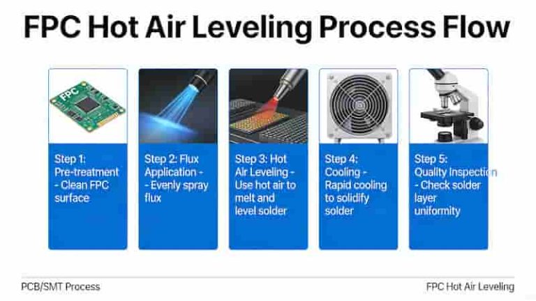
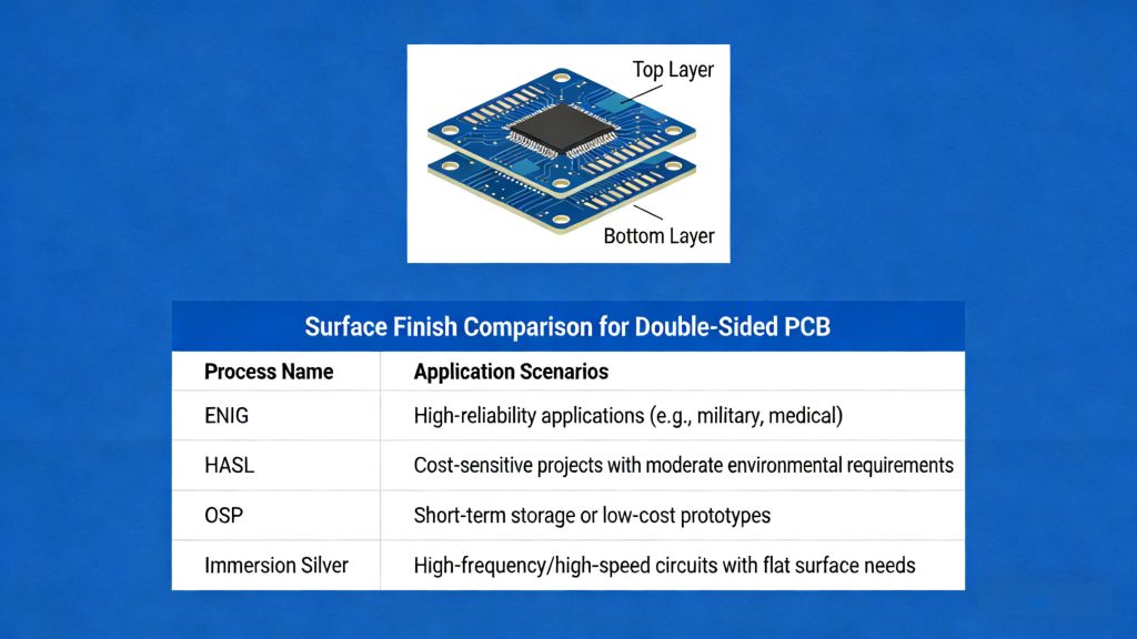
Step 14: Surface Finish Application
Surface finish protects copper pads from oxidation and ensures reliable soldering. Common options (selected by customers based on needs):
- HASL-LF (Lead-Free Hot Air Solder Leveling)
- OSP (Organic Solderability Preservatives)
- ENIG (Electroless Nickel Immersion Gold)
- Immersion Tin / Immersion Silver
Double-Sided PCB Surface Finish Comparison
| Surface Finish | Key Features | Advantages | Best For |
|---|---|---|---|
| HASL-LF | Lead-free tin/copper alloy, hot air leveled | Low cost, excellent solderability, widely available | General-purpose PCBs |
| OSP | Organic compound coating | Flat surface, lead-free, environmentally friendly | Fine-pitch components, short shelf life |
| ENIG | Nickel + gold layer | Excellent corrosion resistance, long shelf life, flat surface | High-reliability PCBs, BGA/QFN |
| Immersion Tin | Thin tin layer deposited chemically | Flat surface, lead-free, good for fine-pitch | High-frequency boards |
| Immersion Silver | Thin silver layer deposited chemically | Excellent conductivity, suitable for high-frequency | RF/microwave boards |
Step 15: Routing (Panel Separation)
The panel (with multiple PCBs) is cut into individual PCBs using a CNC routing machine:
- The routing path follows pre-designed outlines, ensuring clean edges and no damage to the circuit.
Step 16: Flying Probe Test
This is the final electrical test to verify PCB functionality:
- Multiple probes contact the PCB’s test points, passing a small current to check for open circuits (no current flow where it should exist) or short circuits (unwanted current flow).
- Only PCBs that pass the test proceed to packaging.
Step 17: Final Inspection and Vacuum Packaging
- Final inspection: Checks for physical defects (e.g., scratches, solder mask bubbles) and confirms compliance with customer specifications.
- Vacuum packaging: PCBs are sealed in vacuum bags to prevent moisture absorption and dust contamination during storage and shipping.
Double-Sided PCB Manufacturing Process Summary
| Step | Process Stage | Key Activity | Quality Control |
|---|---|---|---|
| 1 | Circuit Design | Schematic creation, component selection | Design review |
| 2 | Layout Design | PCB layout, Gerber file generation | Mirror check for top layer |
| 3 | DFM Check | Manufacturability verification | Trace, hole, pad inspection |
| 4 | Material Selection | FR4 / High-frequency / Metal substrate | Material certification |
| 5 | CCL Cutting | Panel sizing, edge smoothing | Dimensional check |
| 6 | Drilling | Mechanical holes + PTH vias | Hole position accuracy |
| 7 | Electroless Copper | Hole wall copper deposition | Copper thickness check |
| 8 | Photo Imaging | UV exposure + photoresist hardening | Pattern alignment |
| 9 | Pattern Plating | Copper + tin plating (20μm target) | Plating thickness check |
| 10 | Developing & Etching | Remove excess copper | AOI (Step 11) |
| 12 | Solder Mask | Polymer insulation layer | Visual inspection |
| 13 | Silkscreen | Component labels, logos | Print clarity check |
| 14 | Surface Finish | HASL-LF / ENIG / OSP / Tin / Silver | Surface quality check |
| 15 | Routing | CNC panel separation | Edge quality check |
| 16 | Flying Probe Test | Electrical continuity test | Open/short circuit detection |
| 17 | Final Inspection & Packaging | Physical check + vacuum sealing | Final quality audit |
Key Manufacturing Flow Charts
Flow Chart 1: Standard Double-Sided PCB Manufacturing
DFM Check → Cutting of CCL → Drilling → Sinking/1st Copper Plating → Layout (Outer Circuit) → Quality Inspection → Pattern Plating/2nd Copper Plating → Etching → Quality Inspection → Solder Mask → Quality Inspection → Legend Printing → Immersion Tin (or Immersion Gold) → Flying Probe Test → CNC Routing → V-Cut (if required) → Final Inspection → Vacuum Packaging
Flow Chart 2: Double-Sided PCB with Gold Plating
DFM Check → Cutting of CCL → Drilling → 1st Copper Plating → Layout (Outer Circuit) → Quality Inspection → Pattern Plating/2nd Copper Plating → Gold and Nickel Plating → Etching → Quality Inspection → Solder Mask → Quality Inspection → Legend Printing → CNC Routing → V-Cut → Flying Probe Test → Final Inspection → Vacuum Packaging