Filled and capped vias are advanced PCB design techniques that measurably enhance connection reliability. Learn when and why to leverage precision via filling and durable capping to prevent moisture ingress, fractures, and short circuits.
Introduction
As PCBs become more complex with higher component densities and more demanding performance requirements, the reliability of plated through holes, micro vias, blind vias and buried vias, and other via structures is increasingly critical. Tiny cracks, moisture ingress, or material fractures in vias can lead to system failures and costly repairs down the road.
This is why advanced via protection methods such as filled and capped vias are widely used in high‑reliability manufacturing. When properly implemented, filling and capping vias can strengthen connections, prevent oxidation or outgassing, and enable boards to withstand vibration, mechanical shocks, and extreme temperatures.
In this article, we define filled and capped vias, explain their use cases, and outline the measurable reliability improvements you can achieve for global industrial and export PCB projects.
What Are Filled and Capped Vias
Filled vias are plated through holes, microvias, or other via structures filled internally with specialized materials after metallization. Capped vias add an outer protective layer over the via opening to block physical damage and short circuits.
Together, these treatments form a complete Z‑axis protection system for critical PCB interconnects.
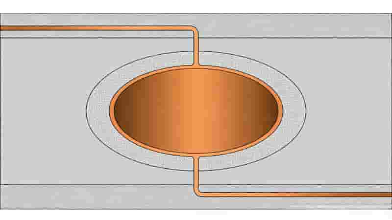
Figure 1: Cross‑Section of a Filled Via for PCB Reliability
Filled Vias: Internal Protection & Reliability
Filled vias block moisture ingress, oxidation, and outgassing inside the via barrel. Common materials include epoxy, resin, and polymer compounds that cure solid to stabilize the via structure.
Precision filling eliminates voids and ensures consistent performance in high‑frequency, high‑temperature, and high‑vibration environments. Properly executed filled vias drastically lower failure rates in industrial and aerospace‑grade PCBs.
Key applications:
- High‑frequency RF and microwave circuits
- Automotive, aerospace, and defense electronics
- Devices exposed to extreme temperatures and humidity
- High‑density designs requiring long‑term stability
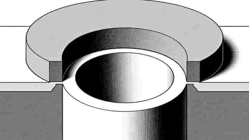
Figure 2: Cross‑Section of a Capped Via for SMT Compatibility
Capped Vias: Surface Shielding & Durability
Capped vias provide a protective layer over the via’s annular ring using solder mask, epoxy, or photoimageable materials. This layer prevents solder wicking, short circuits, and physical damage during SMT assembly and operation.
Capping is especially valuable in high‑density PCBs where nearby components create elevated short‑circuit risks. It also improves thermal cycling stability and resistance to corrosion and mechanical stress.
Top use cases:
- High‑density interconnect (HDI) PCBs
- Consumer and industrial devices with miniaturized layouts
- Products exposed to moisture, dust, and chemical contaminants
- Automated SMT assembly lines requiring stable pad surfaces
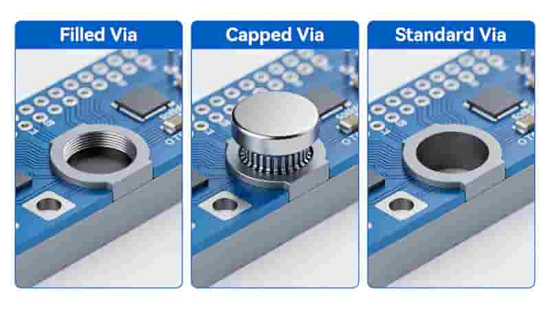
Figure 3: Filled and Capped Vias Combined for Maximum PCB Reliability
Quantifiable Reliability Improvements
Using filled and capped vias delivers measurable performance gains compared to standard vias:
- Thermal Cycle Life: Filled vias withstand 2.8x more thermal cycles than unfilled vias
- Short‑Circuit Reduction: Capped vias lower short risks by ~14% in field applications
- Circuit Density: Protected vias support up to 6.2% higher layout density safely
- Lifespan Extension: Significantly reduced fatigue and fracture in harsh environments
Via Type Comparison
| Via Type | Core Benefit | Best For |
|---|---|---|
| Standard Via | Low cost, simple | Low‑reliability consumer electronics |
| Filled Via | Moisture & outgassing protection | Industrial, aerospace, high‑frequency |
| Capped Via | Short‑circuit & physical protection | HDI, SMT, high‑density boards |
| Filled + Capped Vias | Maximum reliability | Harsh environment, mission‑critical PCBs |
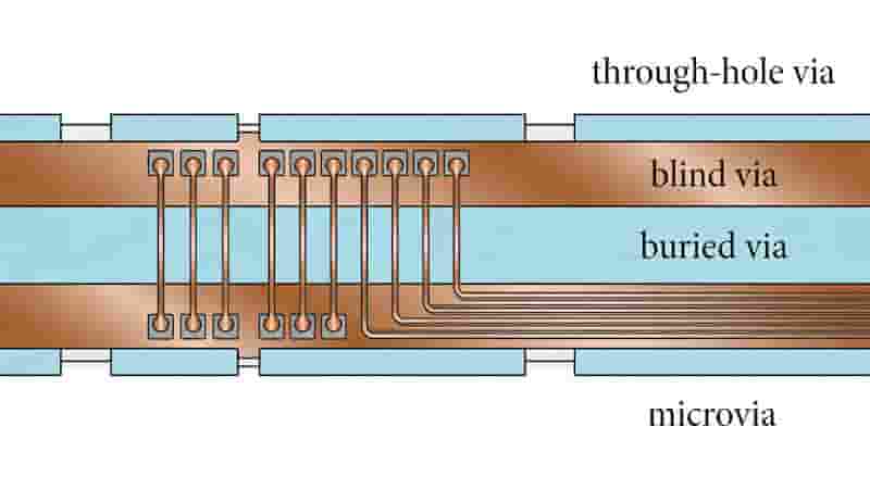
Figure 4: Common Via Types in Modern PCB Design
Conclusion
Filled and capped vias are essential for building robust, long‑life PCBs for industrial, automotive, aerospace, and global export applications. Filling stabilizes internal via structures, while capping protects surface connections. Together, they drastically reduce failures from moisture, thermal stress, vibration, and short circuits.
For high‑performance PCB projects requiring consistent reliability across international markets, filled and capped vias deliver proven, data‑backed improvements.
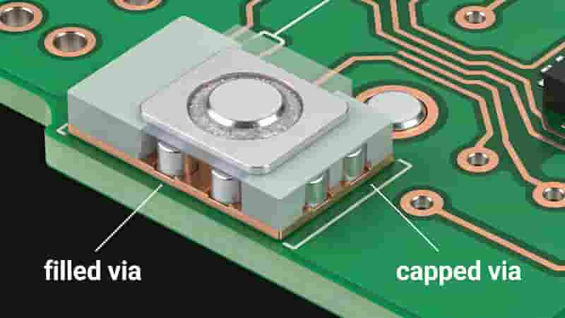
Figure 5: Professional PCB Manufacturing for Filled and Capped Vias
Inquiry & Custom PCB Solutions
We specialize in high‑reliability PCBs with filled and capped vias for industrial and export customers worldwide. Our engineering team supports custom designs, material selection, and optimized processes to meet your performance, quality, and delivery goals.
Contact us today to discuss your PCB project requirements, request a detailed quote, or receive professional design recommendations for filled and capped vias. We provide full support for prototyping and mass production with strict international quality standards.
Get your reliable PCB solution now — send your inquiry and Gerber files for a fast, accurate quote.