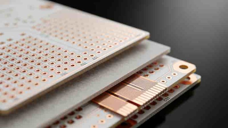
Master how to judge PCB quality with IPC‑aligned inspection tips. Check traces, capacitors, grounding, and testing to ensure durable, high‑performance circuit boards.
PCBs are the foundation of all electronic devices. Learning how to judge PCB quality directly prevents failures, reduces costs, and ensures long‑term reliability for industrial, automotive, medical, and 5G applications. We share 7 professional methods to inspect and validate PCB quality for engineers and global buyers.
1. PCB Trace Quality & Solder Mask
PCB traces carry power and signals across the board. Defects cause short circuits, signal loss, and overheating.
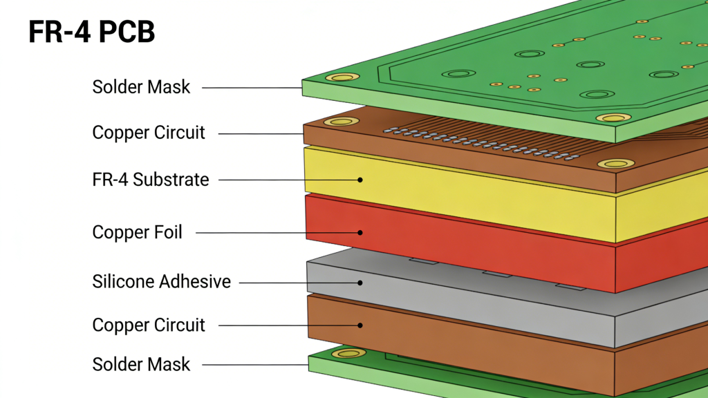
Check uniform solder mask coverage, straight routing, and no sharp bends. High‑quality PCB quality requires traces free of scratches, nicks, or uneven etching.

2. Decoupling Capacitor Placement
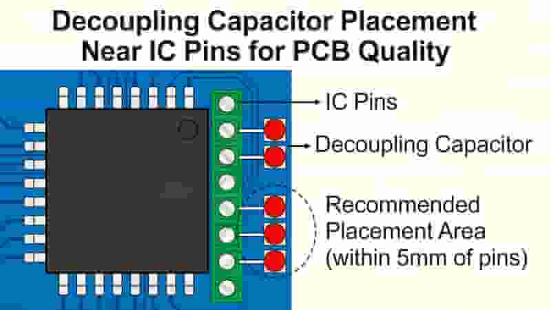
Decoupling capacitors filter high‑frequency noise and stabilize voltage for ICs. Correct placement is critical for PCB quality.
Capacitors must be placed within 1mm of VDD pins. Poor placement causes voltage drops and system instability in processors and high‑speed circuits.
3. Uniform Trace Length for High‑Speed Signals
Matching trace length ensures synchronized signals in DDR, MCU, and high‑speed designs. Mismatch creates timing skew and data errors.
This step is mandatory to maintain true PCB quality for industrial and communication equipment.
4. Antenna Feedline Impedance Matching
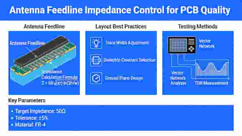
RF and 5G PCBs need 50Ω impedance matching between feedlines and antennas. Mismatch reduces signal range and power efficiency.
Verify with network analyzers to ensure professional PCB quality.
5. Component Placement & Interference Control
Separate analog and digital sections. Space inductors to avoid magnetic coupling. Follow IPC‑7351 for standard PCB quality.
Strategic placement lowers crosstalk and improves thermal performance.
6. Trace Width & Routing Standards
Trace width must match current load per IPC‑2221. Undersized traces overheat; oversized traces waste space.
Correct routing is a foundational part of PCB quality for power and signal boards.
7. Ground Planes & Stability
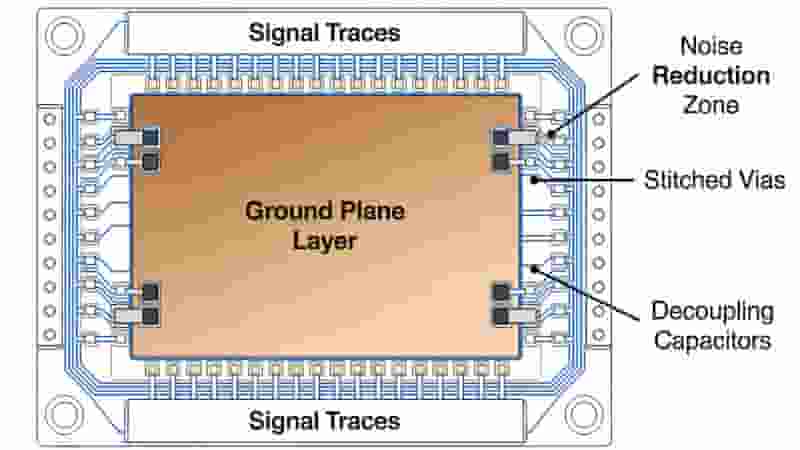
Solid continuous ground planes reduce noise and ensure stable voltage reference. Split analog/digital grounds and connect at the power source.
4‑layer boards greatly improve PCB quality for complex applications.
PCB Testing & Full Quality Control
True PCB quality requires complete testing across design, production, and assembly.
| Test Method | Use Case | Defects Detected |
|---|---|---|
| AOI | Mass Production | Solder, Component, Trace Issues |
| X‑Ray Inspection | BGA, QFN, Hidden Joints | Voids, Cold Joints, Alignment |
| Flying Probe | Prototypes & Low Volume | Open/Short Circuits |
| Functional Test | Final Validation | Real‑World Performance |
Conclusion
Knowing how to judge PCB quality protects your projects from failure and ensures consistent performance. By checking traces, capacitors, grounding, impedance, placement, and testing, you can select reliable PCBs for any application.
We specialize in high‑quality PCB manufacturing with full IPC, RoHS, and ISO compliance for global buyers.
Need Reliable PCB Quality for Your Project?
Contact us for a free quote, custom design review, or sample order. We support global export with fast lead times and strict quality control.