This guide covers the 6 core types of flexible circuit boards, including single-sided, double-sided, multilayer, double access, PTF, and rigid-flex PCBs. Learn their structures, benefits, applications, and how to select the best flex PCB for your industrial, medical, automotive, or aerospace design.
Why Flexible PCBs Matter
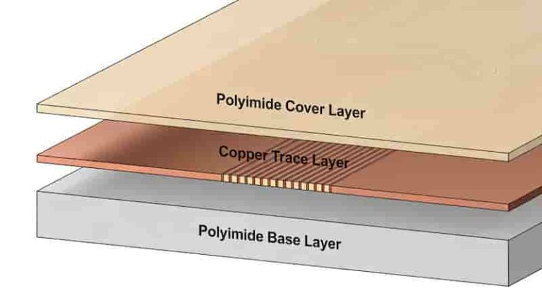
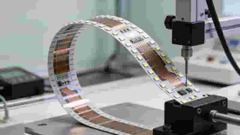
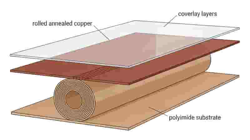
Flexible PCBs (FPCs) are built on bendable substrates like polyimide, offering superior design freedom over rigid PCBs. They reduce weight, save space, improve reliability under vibration, and enable 3D assembly for modern electronics.
- Extreme space optimization for compact devices
- Up to 70% weight reduction vs. rigid PCBs
- Higher reliability in dynamic bending environments
- Support for high-density, high-speed circuits
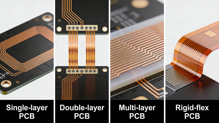
1. Single-Sided Flexible PCB
Single-sided flex PCBs have one conductive copper layer on a flexible dielectric film. They are the most cost-effective and widely used flex PCB type for simple circuits.
Advantages: Low cost, excellent flex life, lightweight, easy assembly.
Applications: Wearables, flexible displays, portable medical devices, sensors.
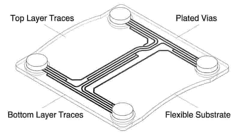
2. Double-Sided Flexible PCB
Double-sided flex PCBs include two copper layers on both sides of the substrate, connected by plated vias. They support higher routing density than single-sided designs.
Advantages: Higher circuit density, compact layout, stable performance.
Applications: Medical instruments, automotive electronics, aerospace controls.
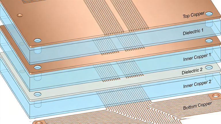
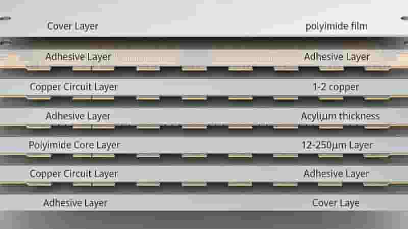
3. Multilayer Flexible PCB
Multilayer flex PCBs consist of 3+ copper layers bonded with thin polyimide films. They deliver ultra-high density and signal integrity for advanced systems.
Advantages: Maximum wiring density, excellent signal control, 3D formability.
Applications: Defense, aviation, high-end medical imaging, 5G equipment.
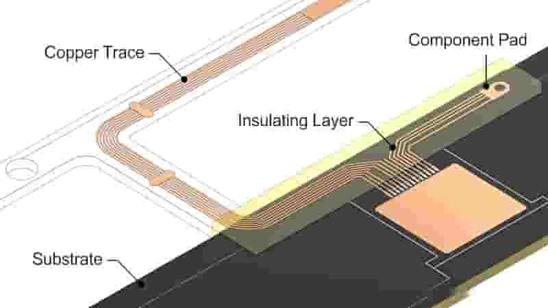
4. Double Access / Back-Bared Flex PCB
This specialized flex PCB uses a single copper layer but exposes traces from both sides for dual-side access, without the cost of a true double-sided board.
Advantages: Lower cost, dual-side testability, good flexibility.
Applications: Disposable medical sensors, IoT modules, consumer electronics.
5. Polymer Thick Film (PTF) Flex PCB
PTF flex PCBs use printed conductive inks on flexible substrates. They are lightweight, eco-friendly, and ideal for low-cost, large-area flexible circuits.
Advantages: Low-cost production, eco-friendly, conformable to curved surfaces.
Applications: Flexible displays, e-textiles, disposable sensors, smart packaging.
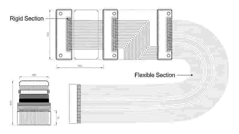
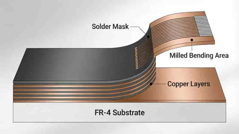
6. Rigid-Flex PCB
Rigid-flex PCBs combine flexible layers and rigid board sections into one integrated circuit. They eliminate connectors and boost reliability in rugged environments.
Advantages: Hybrid stability, high reliability, reduced assembly steps.
Applications: Foldable phones, aerospace, implantable medical devices, automotive ADAS.
Flex PCB Types Comparison Table
| Type | Layers | Cost | Complexity | Best For |
|---|---|---|---|---|
| Single-Sided | 1 | Low | Low | Simple wearables, sensors |
| Double-Sided | 2 | Medium | Medium | Medical, automotive |
| Multilayer | 3+ | High | High | Aerospace, 5G, defense |
| Double Access | 1 | Low-Medium | Medium | IoT, disposable sensors |
| PTF Flex | 1 | Medium | Low-Medium | Flex displays, e-textiles |
| Rigid-Flex | Mixed | High | High | Foldable devices, aerospace |
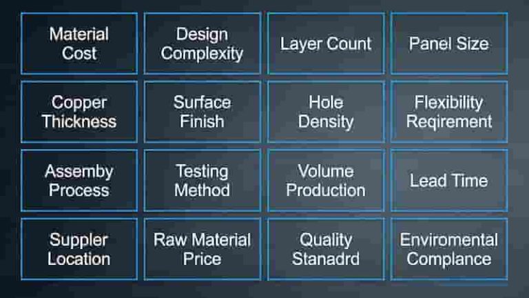
How to Choose the Right Flex PCB Type
Select your flexible circuit board based on design complexity, budget, environment, and application needs:
- Budget & simple circuits: Choose single-sided or double-access flex PCBs
- Medium complexity: Double-sided flex PCBs
- High density & performance: Multilayer or rigid-flex PCBs
- Large-area & low-cost: PTF flexible circuits
Conclusion
Understanding the types of flexible circuit boards helps you select the optimal solution for size, weight, reliability, and cost. Each flex PCB type serves specific design goals, from low-cost sensors to mission-critical aerospace systems.
Request a Custom Flex PCB Quote
We provide professional flex PCB design, prototyping, and mass production for global industrial buyers, engineers, and procurement teams. Contact us today for a free quotation, DFM review, and technical support.
Email us your Gerber files and specifications for an instant, accurate quote.
Prototype PCB Assembly Service – Fast, Reliable & Turnkey Solutions
Professional LED PCB Manufacturing & Assembly Services
Flexible PCB Manufacturing and Assembly: The Complete 2025 Guide
What Is Prototype PCB Assembly
What Are PCB Boards Made Of? Complete Materials Guide for Engineers & Buyers