|

PCB Open Circuit: Causes, Types, Diagnosis & Proven Solutions

4 Types of PCB Open Circuit Diagram Repeated Gap Vacuum Scratched

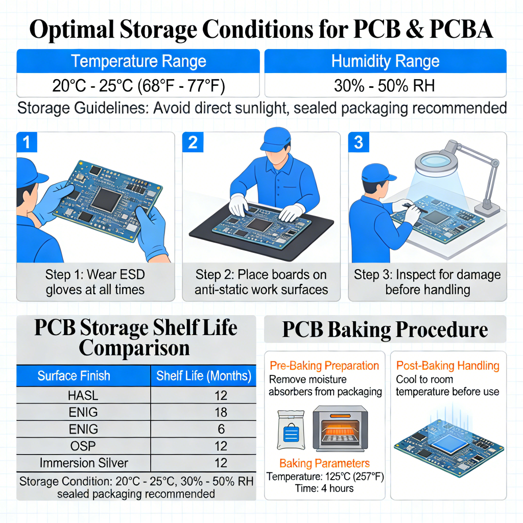
PCB open circuit is one of the most frequent defects in PCB manufacturing, causing production downtime, rework, delivery delays, and quality complaints. This professional guide explains definitions, types, root causes, inspection methods, prevention, and reliable fixes for global electronics buyers and engineers.

What Is a PCB Open Circuit?

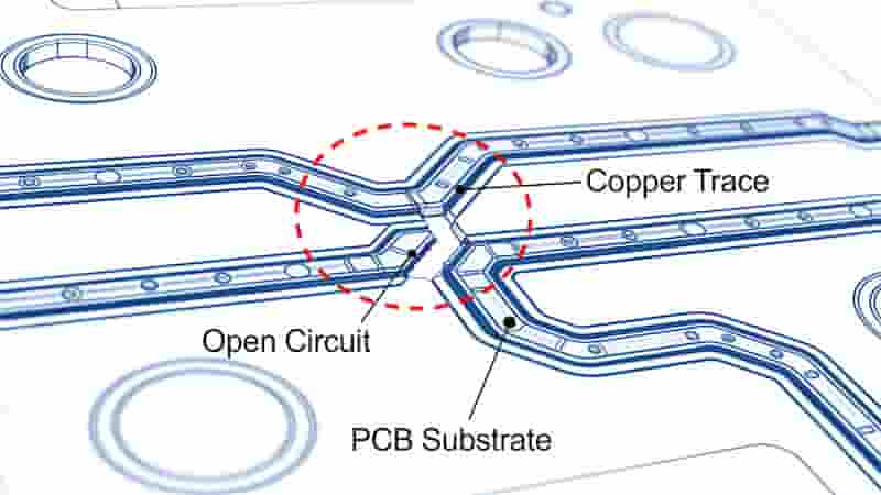
A PCB open circuit is an interruption in the intended conductive path on a printed circuit board. Two points that should be electrically connected become disconnected, blocking current flow and leading to functional failure.

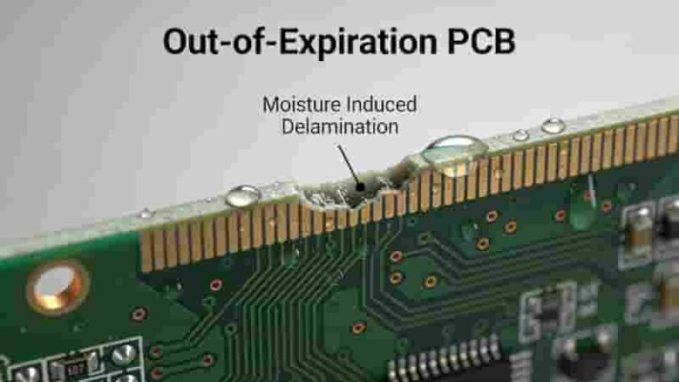
Unlike short circuits, open circuits create gaps, thin traces, or physical breaks in copper circuitry. Common results include dead components, intermittent performance, failed electrical tests, scrapped panels, and delayed shipments.

PCB Open Circuit Definition Diagram Copper Trace Break

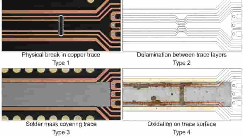
4 Main Types of PCB Open Circuits

1. Repeated Open Circuit

Consistently appears at the same location across a batch, usually caused by damaged or contaminated exposure film.

2. Gap Open Circuit

Visible gap or severely thinned trace, often caused by film defects, dust, or misalignment.

3. Vacuum Open Circuit

Tapered or broken traces caused by trapped air between film and dry film during vacuum exposure.

4. Scratched Open Circuit

Physical damage to copper traces from mishandling, equipment friction, or improper transport.

4 Types of PCB Open Circuit Diagram Repeated Gap Vacuum Scratched

Root Causes of PCB Open Circuits

Material Issues

Low‑quality copper foil, defective dry film, scratched exposure film, or contaminated materials directly cause PCB open circuit failures.

Process Issues

Over‑etching, under‑exposure, improper development, or misaligned imaging lead to incomplete or broken copper paths.

Human Factors

Improper handling, lack of training, or skipped SOPs lead to scratching, bending, or contamination.

Equipment Issues

Poor vacuum contact, worn etching nozzles, unstable UV intensity, or uncalibrated machinery create consistent defects.

PCB Open Circuit Root Causes Material Process Human Equipment

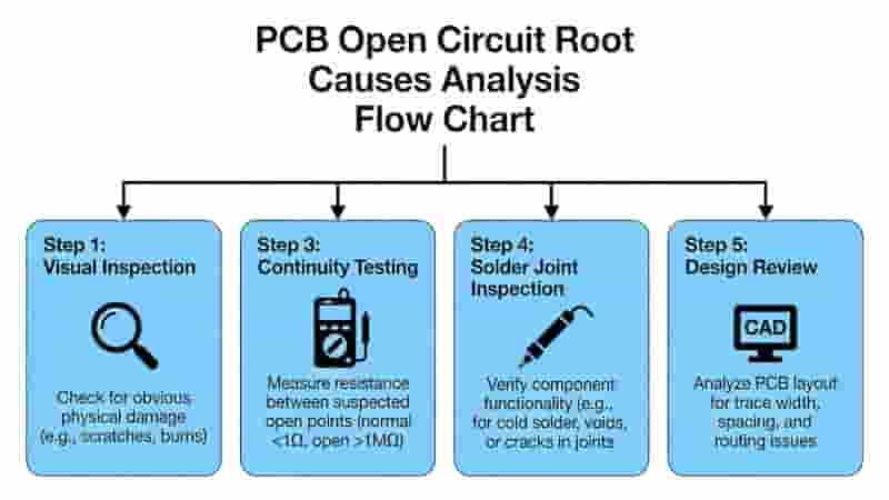
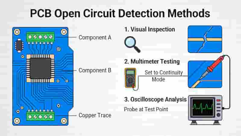
How to Detect PCB Open Circuits

Early detection of PCB open circuit defects reduces rework and scrap costs.

  • AOI (Automated Optical Inspection): High‑speed visual scanning for gaps and thin traces
  • Flying Probe Test: Electrical continuity test for prototypes and low volume
  • X‑Ray Inspection: Detects hidden opens in inner layers of multilayer PCBs
  • Manual Visual Inspection: Magnified check for obvious scratches and gaps
PCB Open Circuit Detection AOI Flying Probe X-Ray Visual Test

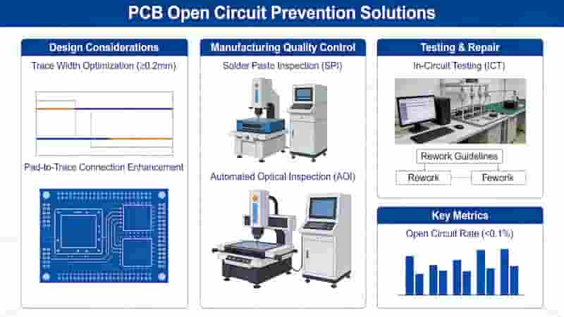
Proven Prevention & Solutions

Control PCB open circuit defects with these industry‑standard methods:

  1. Use high‑purity copper laminates and defect‑free phototools
  2. Calibrate exposure, development, and etching parameters daily
  3. Train operators on proper handling and ESD protection
  4. Maintain vacuum systems and equipment monthly
  5. Implement 100% AOI screening before electrical test
PCB Open Circuit Prevention and Quality Control Solutions

Conclusion

PCB open circuit defects directly reduce yield, increase cost, and damage customer satisfaction. Understanding types, root causes, detection, and prevention allows manufacturers to stabilize quality and improve delivery reliability.

By implementing professional process control and inspection systems, you can minimize open‑circuit failures and produce high‑reliability PCBs for industrial, medical, automotive, and consumer electronics.

Get Reliable PCB Solutions for Your Project

Contact us for professional PCB manufacturing, quality control, defect prevention, and customized production solutions. We support global buyers with stable quality, on‑time delivery, and competitive pricing.

Inquire Now | Get Free Quote

Via-in-Pad Cross Section PCB HDI Technology

Via-in-Pad for Printed Circuit Boards: Complete Technical Guide

Posted on
0 Comments
Via-in-Pad technology places vias directly within surface mount pads to save space, improve routing efficiency, and enhance PCB density for HDI and high-speed designs. What Is Via-in-Pad Technology for PCBs? Before understanding via-in-pad, let’s review common PCB via types: Plated-through holes (PTHs) span the entire board, blind/buried vias connect partial layers, and microvias (~0.1mm) link…
Rigid-Flex PCB structure layers flex core rigid FR4 prepreg coverlay

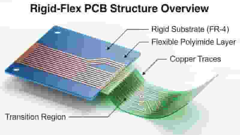
Ultimate Guide to Rigid-Flex PCB Manufacturing: Process, Materials & Quality

Posted on
0 Comments
Rigid-Flex PCB manufacturing integrates flexible circuits and rigid boards to deliver compact, high-reliability interconnect solutions for medical, aerospace, automotive and industrial electronics. This professional guide covers full fabrication flow, material selection, DFM rules, quality control and industry best practices for global engineers and buyers. What Are Rigid-Flex PCBs? Rigid-flex PCBs are hybrid circuit boards that…
PCB dielectric strength HIPOT test equipment and process

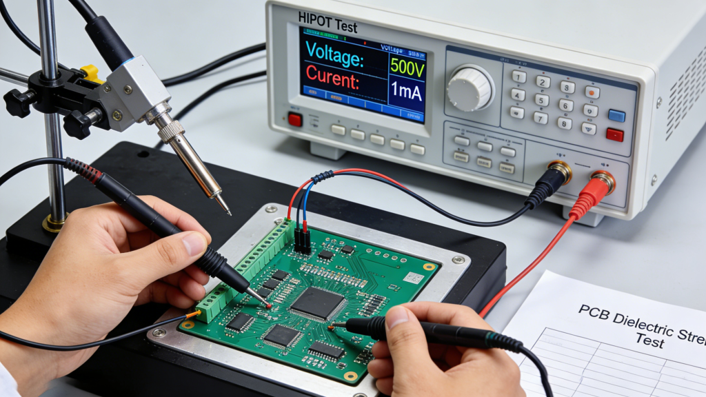
Ultimate Guide to PCB Materials, Dielectric Strength, and Testing in 2025

Posted on
0 Comments
Dielectric strength is critical for PCB reliability, ensuring insulation and safety in high-voltage and high-frequency applications. This guide dives into key PCB materials, their dielectric properties, testing techniques, influencing factors, and practical advice for designing robust circuits. Introduction In the fast-paced world of electronics, a single oversight in PCB design can lead to catastrophic failure—like…
Single Layer Rigid PCB FR-4 Manufacturing

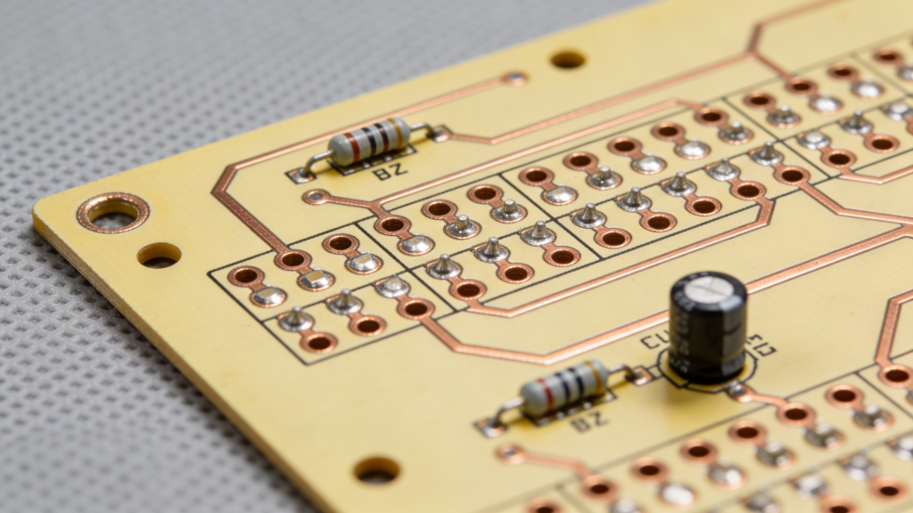
Single Layer PCB Manufacturing | Affordable Single Sided PCBs

Posted on
0 Comments
We provide professional single layer PCB manufacturing and cost-effective single sided PCBs for LED lighting, power supplies, consumer electronics, and industrial equipment. Our ISO & IPC‑certified production ensures stable quality, fast lead times, and free DFM analysis for prototypes and mass production. Single-Layer PCB Definition A single layer PCB (also called single sided PCB) has…
Metal Core PCB cross section structure aluminum copper thermal dielectric layer

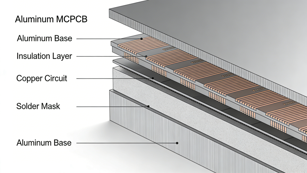
Metal Core PCB (MCPCB) Manufacturing Service in China

Posted on
0 Comments
We are a professional Metal Core PCB manufacturer in China, providing fast MCPCB prototypes and small-batch production with aluminum and copper cores at competitive prices for LED and power electronics. Why Metal Core PCBs (MCPCBs) for High-Power Designs High-power electronic designs face critical thermal management challenges that traditional FR4 PCBs cannot adequately address. Metal Core…
PCB storage environment temperature humidity IPC standard control

How to Store PCB and PCBA? Complete IPC Storage Guidelines

Posted on
0 Comments
Learn PCB storage and PCBA storage best practices to avoid oxidation, ESD, moisture damage, and ensure reliable performance for industrial electronics. PCB storage and PCBA storage are critical for manufacturers and buyers alike. Proper storage prevents damage, maintains solderability, and avoids costly failures during assembly or operation. After production, boards are stored with strict precautions…

FAQ About PCB Open Circuits

A: Damaged exposure film, poor vacuum contact, and physical mishandling are the top three causes.

A: Minor surface opens can be repaired with conductive ink or jumper wires; inner layer opens usually require scrapping.

A: Strict incoming material inspection, stable process control, AOI, and regular equipment maintenance.

Similar Posts