What are pads in PCBs? Learn their key roles in electronics design & manufacturing, explore common pad types, layout considerations, and why they’re critical for reliable PCB performance.
What Are PCB Pads? A Complete Guide to Pad Types and PCB Layout
Introduction
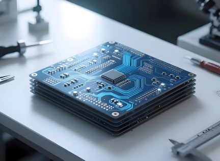
Printed circuit boards (PCBs) are the backbone of modern electronics, connecting components to form functional circuits. Among their critical design elements, PCB pads stand out—they are the key to mounting components and enabling reliable electrical connections. This article breaks down what PCB pads are, their core roles, and why they matter for board design and performance.
A PCB pad is a metallic (typically copper) surface on the circuit board where components are soldered and secured. Beyond physical mounting, pads bridge components to the PCB’s copper traces, ensuring stable signal transmission and power delivery. The right pad size, shape, and placement directly impact manufacturing yield (e.g., reducing solder defects) and long-term device reliability—making them a non-negotiable part of PCB design.
With over 10 years of experience in the PCB industry, we specialize in turning design concepts into high-quality boards—including precise pad fabrication that meets strict industry standards. We offer 24-hour turnaround for simple PCB prototyping (ideal for fast design iteration) and advanced capabilities like HDI, impedance control, and heavy copper (up to 32 layers) for complex projects. Our focus on detail—from pad accuracy to overall board quality—has supported thousands of global customers in bringing their electronics to life.
Types of Pads
In PCB design, pads are categorized by shape and function—each tailored to specific components, assembly methods, and performance needs. Below are the most common types we work with in manufacturing:
1. Pads by Shape
Different shapes address the physical requirements of components (e.g., lead size, mounting space) and help prevent assembly issues like solder bridging:
- Rectangular pads: Standard quadrilateral pads for leaded components (e.g., axial resistors, diodes) — easy to align and cost-effective for mass production.
- Round pads: Circular pads mostly used for through-hole parts (e.g., pin headers) — their symmetry ensures even solder distribution.
- Island pads: Isolated copper regions for surface-mount IC (integrated circuit) contacts — keep individual pins separated to avoid short circuits.
- Polygonal pads: Custom multi-sided pads (e.g., hexagons, octagons) — designed for irregularly shaped components or tight board spaces.
- Oval pads: Elliptical pads for connectors (e.g., USB ports) — longer length accommodates larger contact areas and reduces lead stress.
- Cutout/Void pads: Pads with internal openings — allow venting during soldering (prevents trapped air from causing defects) or fit around board features.
- Specialty shape pads:
- Daisy chain pads: Interlinked flower-shaped pads — used for testing or linking multiple nodes in a sequence.
- Cross-shaped pads: Cruciform (plus-sign) test points — self-centering for probe alignment, ideal for debugging.
- Teardrop pads: Pads with rounded edges — strengthen the connection between pads and traces, avoiding solder bridging or trace cracking.
2. Pads by Function
Functional categories match how pads work with components (e.g., signal transmission, heat dissipation) and follow industry standards like IPC-2221:
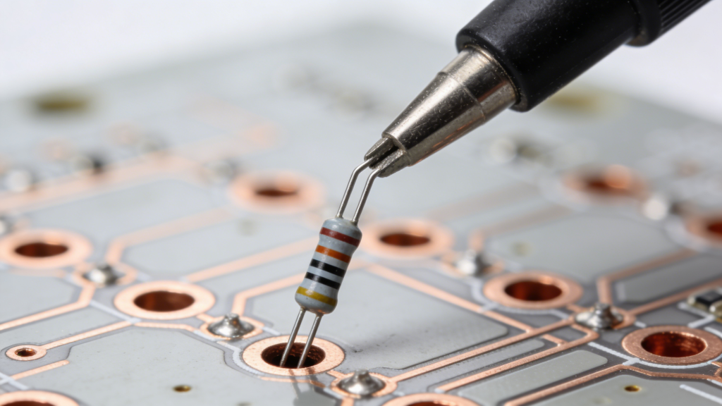
Through-Hole Pads
These are cylindrical pads that let component leads pass through the entire PCB. After inserting leads, they’re soldered to the pad—creating both a strong physical hold and reliable electrical connection.
- Key specs: Per IPC-2221, the “annular ring” (the circular copper ring around the hole) typically ranges from 1.2mm to 2mm (ensures enough solder area).
- Common uses: Leaded components like resistors, capacitors, and connectors—ideal for applications needing high mechanical strength (e.g., industrial devices).
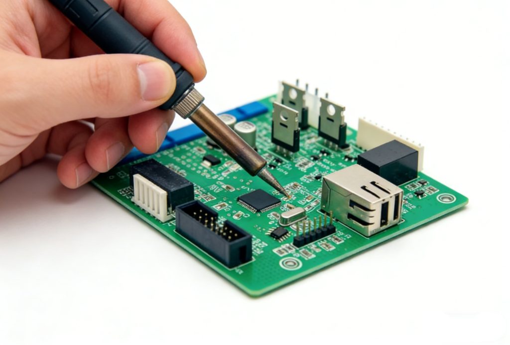
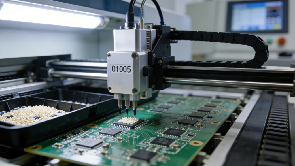
Surface Mount (SMT) Pads
With smaller component sizes came surface mount technology (SMT)—these flat copper pads sit on the PCB surface, no holes needed. They use controlled dimensions and solder masks to form stable joints during reflow soldering (heating solder paste to attach components).
- Key feature: Matches component lead shapes (e.g., “gull wing” or “J-lead” for ICs) to prevent poor soldering.
- Common uses: SMT components like chips, LEDs, and small integrated circuits—perfect for compact devices (e.g., smartphones, wearables).
Thermal Pads
High-power devices (e.g., amplifiers, motor drivers) generate heat—thermal pads transfer this heat to the PCB’s internal copper planes to prevent overheating.
- Design details: Larger pad area (proportional to heat output) plus “thermal vias” (small holes filled with copper) to move heat to inner/bottom PCB layers.
- Common uses: Power-hungry components like microcontrollers and voltage regulators—critical for device longevity.
Test Points
These are simple pads (through-hole or SMT) connected to key circuit “nets” (signal paths)—they let engineers test or troubleshoot the PCB without damaging components.
- Advantage: Require minimal drilling (vs. full holes) and work with standard test probes.
- Common uses: Prototyping and quality checks—speeds up debugging and failure analysis for our clients’ projects.
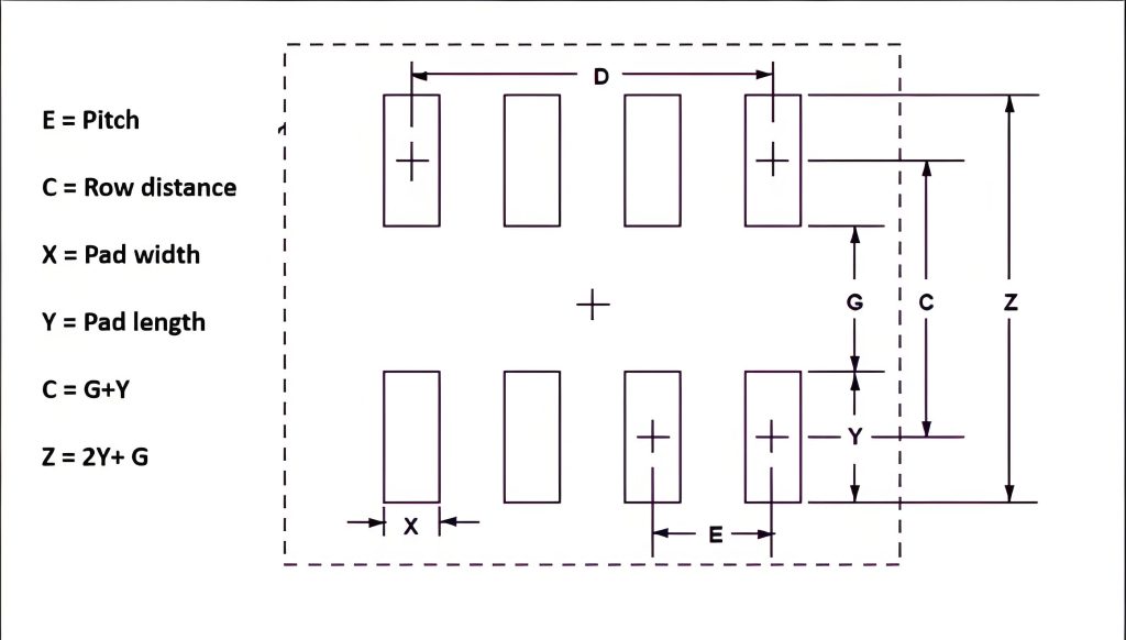
PCB Pad Types Overview Table
| Pad Category | Shape / Type | Key Characteristics | Typical Applications |
|---|---|---|---|
| By Shape | Rectangular | Easy alignment, cost-effective | Axial resistors, diodes |
| Round | Symmetric solder distribution | Pin headers, through-hole components | |
| Island | Isolated copper, prevents short circuits | Surface-mount IC contacts | |
| Polygonal | Custom multi-sided, fits tight spaces | Irregular components | |
| Oval | Elongated, reduces lead stress | Connectors (USB, etc.) | |
| Cutout/Void | Internal openings for venting | Gas release during soldering | |
| Teardrop | Rounded edges, strengthens trace-pad junction | High-reliability designs | |
| By Function | Through-Hole | Drilled hole, strong mechanical bond | Leaded components, industrial equipment |
| SMT (Surface Mount) | Flat, no hole, reflow soldering | Chips, LEDs, compact devices | |
| Thermal | Large area + thermal vias, dissipates heat | Power ICs, voltage regulators | |
| Test Point | Minimal drilling, probe-compatible | Debugging, quality assurance |
Our Capabilities for Pad Fabrication
We handle reliable manufacturing of all the pad types above—from standard through-hole pads to intricate SMT pads and large thermal pads. Our precision machinery (e.g., laser drilling, automated solder mask application) and strict quality control (checking pad dimensions, alignment) ensure consistency across every board—whether it’s a small prototype or high-volume production run.
Role of Pads in PCB Layout
The layout of pads on a PCB is critical for both design success and smooth manufacturing—they act as the “bridge” between component placement, trace routing, and final assembly. Below are the key roles pads play in the layout process:
1. Guiding Component Placement
PCB designers first place components strategically, based on factors like circuit topology (how the circuit connects), high-speed signal paths, and heat dissipation needs. Every component has a “footprint” (a digital template that defines pad positions), so pad layout directly mirrors component layout to ensure proper mounting.
- Key standard: We follow design rules that maintain adequate spacing between pads (e.g., avoiding overlap) to prevent assembly errors like solder short circuits.
2. Enabling Trace Routing
Pads are the “endpoints” for copper traces—they let traces connect components across the board, following the circuit schematic. Careful pad positioning reduces the need for long, winding traces, which in turn minimizes “crosstalk” (unwanted signal interference between traces).
- Practical benefit: This not only improves signal integrity but also simplifies routing, saving time in the design process—something we prioritize when supporting our clients’ layout work.
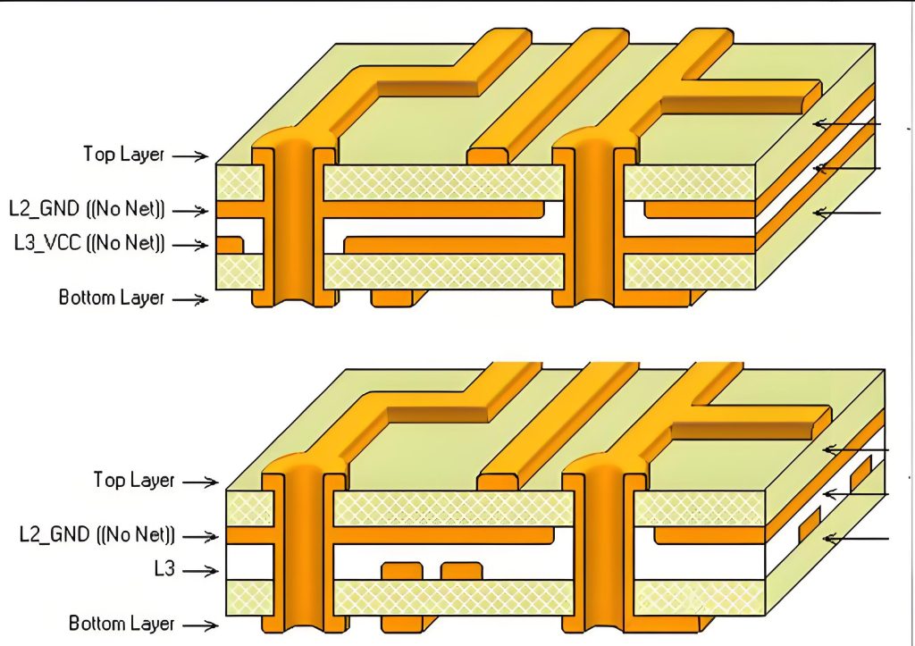
3. Supporting Via Transitions
Vias (small holes that connect traces between PCB layers) need to work with pads to avoid shorts. Specifically, via barrels (the metalized inner walls of vias) must fully overlap with pads, while maintaining clear space around pads.
- Our practice: When advising on layout, we remind designers to align pad locations with planned via transitions—this ensures reliable interlayer connectivity and avoids rework during manufacturing.
4. Ensuring Smooth Assembly
Pad dimensions and tolerance (allowable size variation) directly impact three key assembly steps: solder paste application (how much paste sticks to pads), component placement (whether parts sit correctly), and soldering (how well joints form).
- Critical outcome: Optimized pad designs (matching IPC standards) maximize finished product yield (fewer defective boards) and long-term reliability—something we verify through our in-house quality checks during fabrication.
Our Support for Pad Layout
With years of PCB manufacturing experience, we don’t just produce boards—we also provide tailored layout recommendations for pad arrangements, based on our clients’ specific needs (e.g., high-speed designs, power boards). Our precision fabrication capabilities ensure that pads meet stated specifications (size, spacing, tolerance) with high consistency, from prototype to mass production.
Significance of Pads in PCBs
Pads are among the most critical elements in PCB design—without them, components can’t attach to the board or connect electrically. Their significance spans four key areas, directly impacting a PCB’s performance, durability, and manufacturability:
1. Enabling Core Electrical Functionality
Pads act as the “connection point” between components and the PCB’s copper traces. This lets signals (e.g., data) and power flow between different parts of the circuit—without properly designed pads, the circuit would fail to work.
- Key detail: We prioritize pad accuracy in manufacturing because even small deviations (e.g., misaligned pads) can disrupt electrical connectivity, leading to device malfunctions.
2. Providing Mechanical Stability
When components are soldered to pads, the solder joint creates a strong physical bond. This keeps components securely attached to the PCB, even when exposed to vibration (e.g., in industrial machines) or minor shocks (e.g., accidental drops).
- Practical impact: For our clients designing durable devices (like automotive or industrial electronics), well-made pads are essential to avoid component fall-off over time.
3. Supporting Thermal Management
High-heat components (e.g., power amplifiers, motor drivers) need a way to dissipate heat—and pads play a key role here. Specialized thermal pads connect these components to the PCB’s internal copper planes, transferring heat away to prevent overheating.
- Our approach: We fabricate enlarged thermal pads (custom-sized based on a component’s heat output) to ensure effective cooling, which extends the device’s lifespan.
4. Simplifying Manufacturability
The size, shape, and position of pads directly affect how easy (or difficult) a PCB is to assemble. Precise pad dimensions ensure:
- Solder paste adheres correctly (no too much/too little paste),
- Machines can place components accurately,
- Soldering processes go smoothly (fewer defects).
- Why it matters: For us, well-designed pads mean higher production yields (fewer faulty boards) and faster turnaround for our clients.
Summarizing Pad Significance
In short, PCB pads do four critical things: make circuits work (electrical), keep components secure (mechanical), prevent overheating (thermal), and streamline production (manufacturing). With our advanced fabrication capabilities, we help customers fully leverage optimized pad designs—turning their PCB concepts into reliable, high-performance products.
Conclusion
While small in size, PCB pads are foundational to a board’s architecture—they’re the critical link that integrates components both physically and electrically. Optimizing pad design and layout isn’t just a detail; it’s what ensures smooth assembly and long-term reliability for electronic devices.
This article broke down the essentials of PCB pads, from their types and layout rules to their far-reaching significance. The key takeaways are clear:
- Pads act as the soldered bridge between component pins and PCB traces, enabling both signal/power flow and mechanical stability;
- Different pad shapes (e.g., round, rectangular) and types (through-hole, SMT) are tailored to specific components and assembly needs;
- Pad details—size, positioning, and spacing—directly impact how easy a board is to manufacture and how well it performs long-term.
At every stage, we’re committed to fabricating PCBs with consistently high-quality, dimensionally accurate pads that match your exact specifications. Our goal is simple: to turn your pad designs into functional, reliable boards that meet your project objectives. With nearly a decade of PCB manufacturing expertise, we’ve supported over 10,000 customers globally—from streamlined prototyping to full-scale production. Let’s work together to bring your electronics vision to life.
Related Reading
What is FR-4 Material in PCB Fabrication? The Complete Engineering Guide
What is FR-4 Material in PCB Fabrication? Complete Engineering Guide

What is a Surface Mount Device or SMD Component Package?
Turnkey PCB Assembly Services | Full & Partial Solutions
Through-hole PCB Assembly Service | IPC Certified THT PCBA Solutions