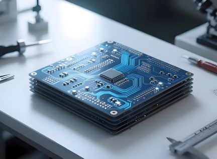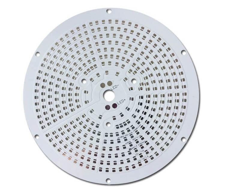
We provide professional BGA PCB manufacturing, precision assembly, rework, reballing, and full turnkey solutions for global industrial, automotive, medical, and telecom customers. Our ISO & IPC-compliant processes ensure high yield, reliability, and fast delivery from prototypes to volume production.
What Is BGA (Ball Grid Array) and Why It Matters for Your PCB?
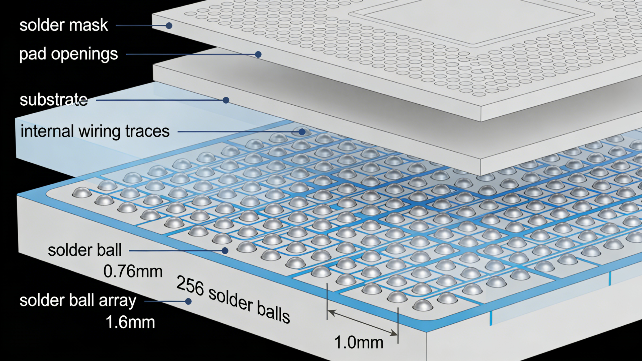
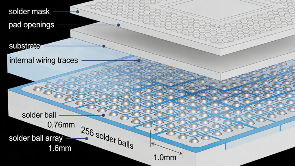
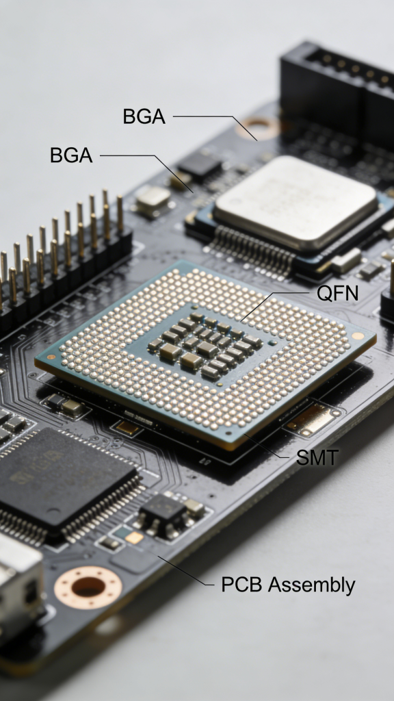
A ball grid array (BGA) is a high-density surface-mount package that uses an array of solder balls on the underside of the component instead of traditional leads. It is widely used in advanced electronics such as processors, FPGAs, ASICs, memory, and high-speed communication devices where compact size and high I/O counts are required.
- Higher I/O density in a smaller footprint compared to QFP and other leaded packages.
- Improved electrical performance and signal integrity for high-speed, high-frequency designs.
- Better thermal performance and heat dissipation through the solder ball array.
- Increased mechanical reliability with controlled reflow and proper BGA PCB design.
Today, BGA PCB assemblies are standard in smartphones, networking equipment, automotive control units, and industrial automation. Choosing the right manufacturing partner ensures long-term reliability and consistent yield.
BGA PCB Manufacturing & Assembly Capabilities
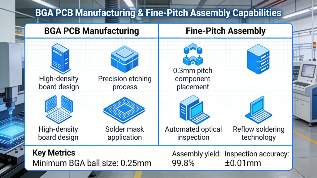
We provide comprehensive BGA PCB manufacturing and assembly services for fine-pitch, high-density designs. Our capabilities cover standard BGA, micro BGA, and complex multi-BGA boards with advanced SMT and 100% X-ray inspection.
| Item | Capability |
|---|---|
| BGA Package Types | PBGA, CBGA, FBGA, micro BGA, stacked BGA, PoP |
| Minimum BGA Pitch | Down to 0.25 mm (fine-pitch & µBGA) |
| PCB Layers | Up to 40 layers for HDI BGA PCB |
| Min Trace/Space | 2.5/2.5 mil (0.063 mm) with HDI stack-ups |
| Via Technology | Microvias, via-in-pad (filled & capped) |
| Surface Finishes | ENIG, ENEPIG, immersion tin, HASL, gold |
| Inspection | 100% X-ray, 3D AOI, ICT, functional test |
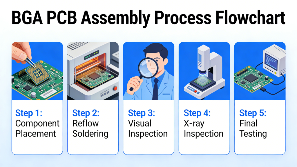
BGA PCB Manufacturing & Assembly Process
Our controlled end-to-end process ensures reliable BGA PCB solder joints and consistent production yield from DFM review to final inspection.
1. Engineering Review & DFM Check
We review Gerber, BOM, and placement files to optimize BGA pad design, fan-out, via-in-pad, and thermal layout for manufacturability and reliability.
2. HDI PCB Fabrication
Multilayer and HDI BGA PCB production with tight registration, microvias, and premium surface finishes for consistent solderability.
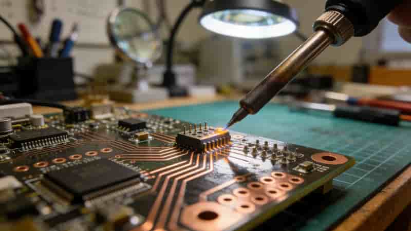
3. Solder Paste Printing & BGA Placement
High-precision stencil printing and automated placement with ±25 µm accuracy for fine-pitch devices.
4. Reflow Soldering
Customized thermal profiles prevent head-in-pillow, voids, and bridging for stable BGA PCB joints.
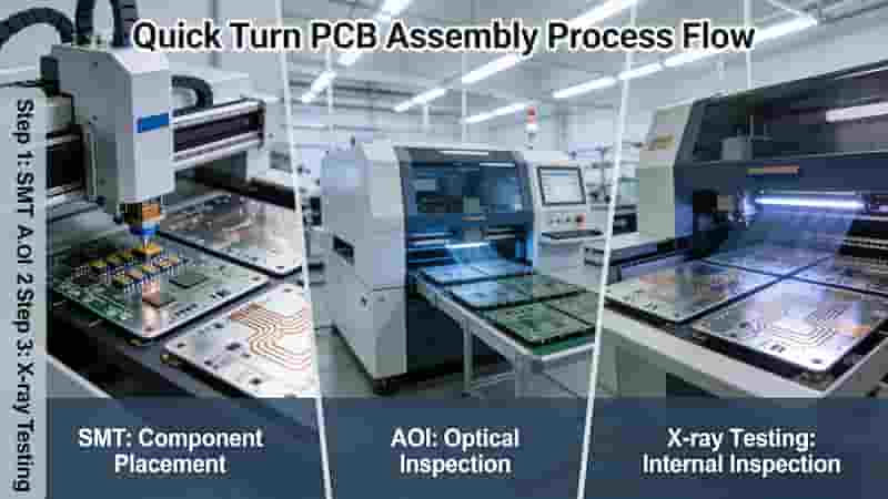
5. 100% X-Ray & AOI Inspection
Full X-ray inspection of hidden solder joints; 3D AOI verifies placement and visible solder quality.
6. Testing & Shipping
ICT, flying-probe, and functional testing available; ESD-safe packaging for global delivery.
BGA PCB Design & DFM Guidelines
Optimize your layout for BGA PCB assembly success with our proven design rules to avoid respins and assembly failures.
- Use NSMD pads for better solder joint reliability and consistent dimensions.
- Apply dog-bone fan-out for ≥0.65 mm pitch; via-in-pad for ≤0.4 mm ultra-fine pitch.
- Fill and cap vias on BGA pads to prevent solder wicking and voids.
- Maintain proper solder mask clearance to avoid bridging.
- Add thermal vias under high-power BGAs to improve heat dissipation.
- Keep clearance around BGAs for X-ray inspection and rework access.
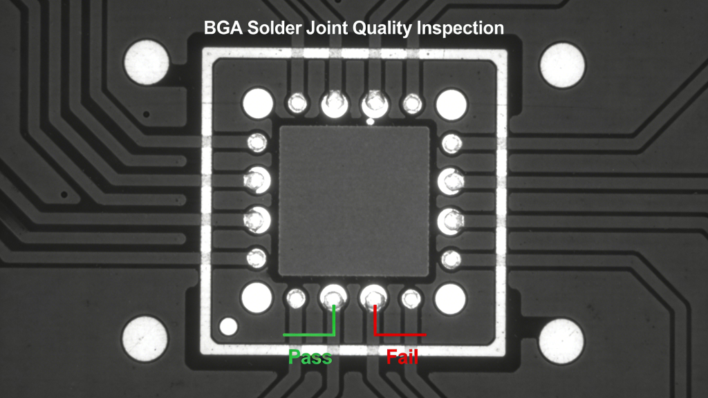
BGA PCB Quality Control & Inspection
Quality is critical for BGA PCB because solder joints are hidden. Our inspection system eliminates latent defects.
100% X-Ray Inspection
Detects voids, opens, shorts, misalignment, and head-in-pillow defects invisible to optical tools.
3D AOI & Process Control
Validates component placement, polarity, and solder fillets; real-time reflow profile monitoring ensures consistency.
Electrical & Reliability Testing
ICT, flying-probe, functional test, burn-in, and environmental screening available for high-reliability BGA PCB projects.
Industries & Applications for BGA PCB Assemblies
Our BGA PCB solutions serve high-performance industries demanding density, speed, and reliability:
- Consumer Electronics: Smartphones, tablets, gaming, IoT devices
- Networking & Telecom: Routers, switches, 5G equipment, optical modules
- Automotive: ECUs, ADAS, infotainment, vehicle connectivity
- Industrial Automation: PLCs, drives, robotics, machine vision
- Medical & Instrumentation: Diagnostics, imaging, precision tools
BGA PCB Pricing, Lead Time & Quote Requirements
Cost and lead time for BGA PCB depend on layer count, BGA pitch, HDI structure, quantity, and testing.
Typical Lead Times:
- Prototypes: 7–10 working days
- Complex HDI BGA boards: 10–15 working days
- Volume production: confirmed per project
To request a quote, provide:
- Gerber/design files (including drill and stack-up)
- BOM with part numbers
- Pick-and-place/XY data
- Assembly notes and test requirements
- Order quantity and target lead time

Summary
We deliver full-service BGA PCB manufacturing and assembly with fine-pitch capability, HDI expertise, 100% X-ray inspection, and end-to-end quality control. From prototype to volume production, we support global buyers with reliable, cost-effective, and on-time BGA PCB solutions for industrial, automotive, medical, and telecom applications.
Request Your BGA PCB Quote Today
Get DFM review, competitive pricing, and fast lead time for your BGA PCB project.
Get BGA PCB Quote
SMT PCB Assembly Services for Prototypes & Production
What Is the Difference Between PTH and Via in PCBs?
How to Choose the Right Quick Turn PCB Assembly Manufacturer
What is a Surface Mount Device (SMD) Component Package?
Through-hole PCB Assembly Service | IPC Certified THT PCBA Solutions