We provide professional BGA PCB manufacturing, precision assembly, advanced rework, and full testing for high-reliability electronics. Our ISO/IPC-certified processes support prototypes to mass production for global industrial buyers, engineers, and procurement teams.
What Is BGA (Ball Grid Array) and Why It Matters for Your PCB?
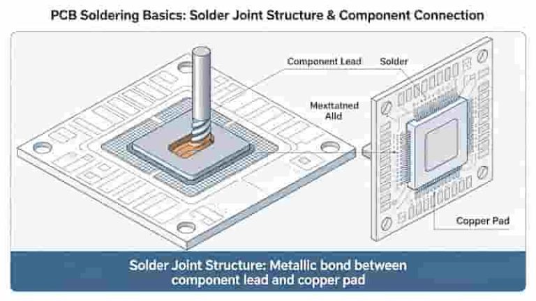
A ball grid array (BGA) is a high-density surface-mount package that uses an array of solder balls on the underside of the component instead of traditional leads. It is widely used in advanced electronics such as processors, FPGAs, ASICs, memory, and high-speed communication devices where compact size and high I/O counts are required.
- Higher I/O density in a smaller footprint compared to QFP and other leaded packages.
- Improved electrical performance and signal integrity for high-speed, high-frequency designs.
- Better thermal performance and heat dissipation through the solder ball array and internal structure.
- Increased mechanical reliability when assembled with a controlled reflow process and proper PCB design.
Today, BGA packages are standard in smartphones, networking equipment, automotive control units, industrial automation systems, and many other compact, high-performance electronic products. Choosing the right BGA PCB manufacturing and assembly partner is critical to ensure long-term reliability and consistent yield.
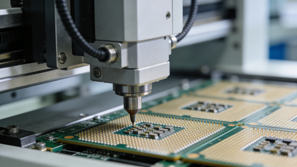
BGA PCB Manufacturing & Assembly Capabilities
We provide comprehensive BGA PCB manufacturing and assembly services for fine-pitch, high-density designs. Our capabilities cover standard BGA, micro BGA, and complex multi-BGA boards, backed by controlled PCB fabrication, advanced SMT lines, and 100% X-ray inspection of all BGA solder joints.
| Item | Capability (Typical Values / Range) |
|---|---|
| BGA package types | PBGA, CBGA, FBGA, micro BGA, stacked BGA, PoP (package-on-package) |
| Minimum BGA pitch | Down to 0.25 mm (fine-pitch BGA and µBGA) |
| Supported PCB layers | Up to 40 layers for BGA-based high-density multilayer PCBs |
| Board thickness range | Typically 0.4 mm – 3.2 mm (custom thickness on request) |
| Min trace/space for BGA breakout | Down to 2.5/2.5 mil (0.063/0.063 mm) with HDI stack-ups |
| Via technology | Through-hole, laser-drilled microvias, stacked and staggered microvias, via-in-pad (filled and capped) for fine-pitch BGAs |
| Surface finishes | ENIG, ENEPIG, immersion tin, immersion silver, lead-free HASL, hard gold / soft gold |
| BGA assembly volume | Prototypes (1–50 pcs), small to medium batches, and mass production |
| Placement accuracy | High-speed SMT placement with ±25 µm accuracy (3σ) for fine-pitch BGAs |
| Inspection & testing | 100% X-ray inspection for all BGAs, 3D AOI, ICT and functional testing |
| Rework & reballing | Precision BGA rework, replacement, and reballing services with dedicated stations |
With these capabilities, we can reliably handle complex BGA-based PCBs from early prototypes to stable volume production, while our engineering team supports you with DFM reviews and optimized processes for consistent quality and yield.
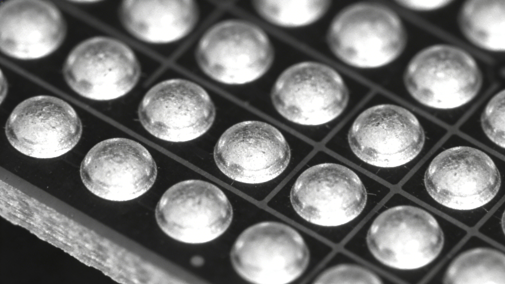
BGA PCB Manufacturing & Assembly Process
To ensure reliable BGA solder joints and consistent yield, we follow a tightly controlled end-to-end process for BGA PCB manufacturing and assembly. From DFM review and HDI fabrication to optimized reflow profiles and 100% X-ray inspection, every step is engineered for quality.
Step 1 – Engineering Review & BGA DFM Check
Our engineers start with a detailed review of your Gerber, BOM, and pick-and-place files, focusing on BGA pad design, fan-out strategy, via-in-pad structures, solder mask clearances, and thermal considerations. We provide DFM feedback when needed to improve manufacturability, yield, and long-term reliability of your BGA-based designs.
Step 2 – HDI PCB Fabrication for BGA Designs
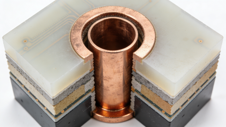
For BGA and fine-pitch packages, we manufacture multilayer and HDI PCBs with controlled layer registration, tight trace/space, microvias, and via-in-pad structures. Advanced lamination, drilling, copper plating, and surface finishes such as ENIG or ENEPIG are used to provide flat, reliable BGA pads with excellent solderability.
Step 3 – Solder Paste Printing & BGA Placement
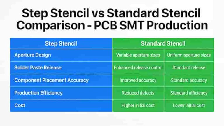
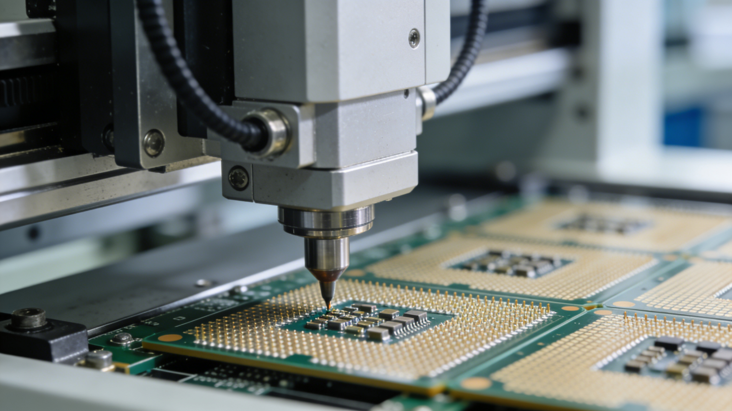
Using high-precision stencil printing and SPI (solder paste inspection), we ensure accurate paste volume and alignment on all BGA pads. Automated SMT lines then place BGAs and other fine-pitch components with high accuracy, minimizing placement variation and potential solder defects.
Step 4 – Reflow Soldering with Optimized Profiles
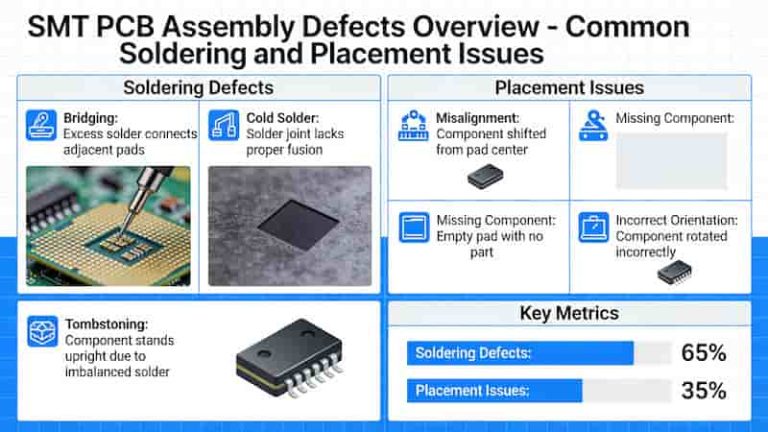
We develop and control reflow profiles matched to your PCB stack-up, BGA package type, and solder paste to achieve proper wetting and collapse of each solder ball. Careful thermal management helps prevent common BGA defects such as head-in-pillow, voids, opens, and bridging.
Step 5 – 100% X-Ray Inspection & AOI
All BGA solder joints are inspected using high-resolution X-ray systems to detect voids, shorts, opens, misalignment, and other hidden defects. In addition, 3D AOI checks component placement, polarity, and solder fillets on visible joints to ensure overall assembly quality.
Step 6 – Testing, Packaging & Shipping
On request, we perform ICT and functional testing according to your test procedures to verify board performance before shipment. Finished BGA PCB assemblies are cleaned, packaged with ESD-safe materials, and shipped worldwide with proper handling instructions to protect sensitive components and solder joints.
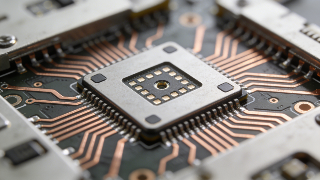
BGA PCB Design & DFM Guidelines
Reliable BGA PCB assembly starts with a manufacturable PCB design. To help you avoid costly respins and BGA solder issues, our engineering team provides DFM support and practical design guidelines for BGA pad geometry, fan-out, via structures, and solder mask design.
1. BGA Pad Design & Land Pattern
- Follow the component manufacturer’s recommended land pattern for each specific BGA package.
- Use non-solder mask defined (NSMD) pads for most BGAs to achieve better solder joint reliability.
- Ensure adequate pad-to-pad spacing to accommodate solder mask and prevent bridging between neighboring balls.
2. Fan-Out Strategy & Escape Routing
- For BGA pitches ≥ 0.65 mm, traditional dog-bone fan-out with vias placed just outside the pad ring is typically sufficient.
- For 0.4–0.5 mm pitch BGAs, consider using microvias in the dog-bone or between pads, combined with HDI stack-ups to escape inner rows.
- For ultra-fine pitch (0.3–0.25 mm), via-in-pad with filled and capped vias is often required to route signals while maintaining controlled impedance and manufacturability.
3. Via-in-Pad & Solder Mask Considerations
- When using via-in-pad for BGA, ensure vias are properly filled and capped to prevent solder wicking and voids under the balls.
- Avoid open through-holes on BGA pads; instead, use tented or covered vias away from pads if via-in-pad is not required.
- Carefully define solder mask openings to balance solder spread, avoid mask slivers, and maintain sufficient dam between adjacent pads.
4. Stack-Up, Power Integrity & Thermal Management
- Use solid reference planes under BGA areas to control impedance and reduce noise for high-speed signals.
- Place decoupling capacitors as close as possible to BGA power/ground balls, typically on the back side directly under the BGA with short via connections.
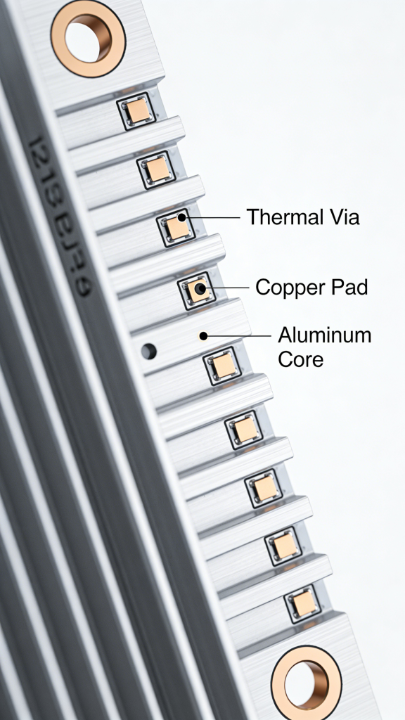
- Add thermal vias under hot BGAs to spread heat into internal copper planes and improve overall thermal performance.
5. Design for Inspection & Rework
- Maintain sufficient clearance around BGA to allow effective X-ray inspection and potential rework operations.
- Avoid placing tall components too close to BGA edges, which can shadow X-ray images or interfere with hot-gas nozzles on rework equipment.
- Clearly mark BGA pin 1 and orientation on the silkscreen to reduce assembly and debugging errors.
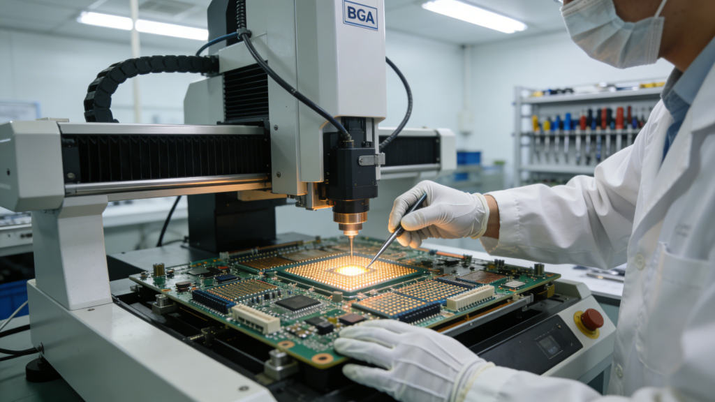
BGA Quality Control & Inspection
Because BGA solder joints are hidden under the package body, robust inspection and process control are essential to avoid latent defects. We combine optimized reflow profiles, 100% X-ray inspection, 3D AOI, and optional electrical testing to ensure that every BGA PCB assembly meets your reliability requirements.
1. 100% X-Ray Inspection for All BGAs
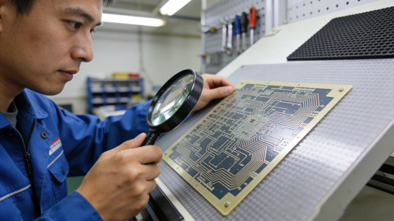
Every BGA on your boards is inspected using high-resolution X-ray systems to reveal hidden solder joints. X-ray images allow our technicians to detect voids, insufficient solder, opens, shorts, head-in-pillow defects, misalignment, and other issues that cannot be seen with optical inspection alone.
2. 3D AOI for Overall Solder Quality
In addition to X-ray, 3D AOI checks the height, shape, and position of visible solder joints and components across the entire PCB. This helps confirm correct component values and polarity, solder fillet quality, and placement accuracy for QFNs, QFPs, connectors, and passives surrounding your BGAs.
3. Controlled Reflow Profiles & Process Monitoring
We develop and monitor tailored reflow profiles based on your PCB thickness, copper weight, and BGA package types to achieve consistent solder joint formation. Continuous process control including temperature profiling, solder paste inspection, and placement verification reduces process variation and improves long-term field reliability.
4. Electrical Testing & Reliability Options
On request, we can perform in-circuit testing (ICT), flying-probe testing, and functional testing according to your test procedures to catch defects that visual inspection cannot detect. For high-reliability applications, we can also support additional reliability measures such as burn-in or environmental stress screening in cooperation with your engineering team.
Industries & Applications for BGA PCB Assemblies
BGA packages are used across many high-performance electronic products that demand compact size, high I/O density, and reliable high-speed interconnects. We support BGA PCB manufacturing and assembly for a wide range of industries and end applications.
Consumer Electronics
BGA-based PCBs are widely used in smartphones, tablets, gaming consoles, set-top boxes, and smart home devices, where compact form factors and high processing performance are critical. We can support rapid prototyping and production of consumer boards with complex SoCs and memory BGAs.
Networking & Telecom
Routers, switches, base stations, and optical network equipment rely on high-pin-count BGAs for processors, FPGAs, and high-speed interfaces. Our HDI PCB fabrication and fine-pitch BGA assembly help maintain signal integrity and power integrity in demanding telecom environments.
Automotive & Transportation
Modern vehicles use BGAs in infotainment systems, ADAS controllers, ECUs, and connectivity modules that must operate reliably under wide temperature ranges and vibration. Our controlled processes and robust inspection support the stringent quality expectations of automotive and transportation applications.
Industrial Control & Automation
Industrial controllers, PLCs, motor drives, and robotics platforms often integrate BGAs for high-performance CPUs, FPGAs, and communication interfaces. We provide BGA PCB assemblies designed for long service life and stable operation in harsh industrial environments.
Medical & Instrumentation
Diagnostic equipment, imaging systems, and laboratory instruments require compact, reliable PCBs with high processing and data acquisition capabilities, often using BGA and micro BGA packages. We support low- to medium-volume BGA assemblies for instrumentation and specialized electronics.
BGA PCB Pricing, Lead Time & Quote Requirements
BGA PCB manufacturing and assembly costs depend on board complexity, BGA pitch and count, HDI structures, component mix, testing requirements, and requested lead time. We offer competitive pricing for both rapid prototypes and volume BGA production, with flexible options to match your schedule and budget.
Typical Lead Time for BGA PCB Assembly
- Prototypes and small runs: Typically 7–10 working days after all materials and data are confirmed.
- Complex HDI BGA boards (≥ 10 layers, fine-pitch via-in-pad): Typically 10–15 working days.
- Volume production: Standard lead times agreed case-by-case based on order quantity and supply chain.
Key Cost Drivers for BGA PCB Manufacturing & Assembly
- PCB complexity: layer count, HDI structure, microvias, via-in-pad, controlled impedance stack-up.
- BGA details: number of BGA components per board, ball count, minimum pitch, and required X-ray inspection level.
- Components & sourcing: BOM mix (standard vs. special parts), supply chain availability, and consigned parts.
- Testing & quality requirements: ICT, functional testing, burn-in or higher IPC class standards.
- Lead time: expedited or quick-turn services will typically carry a premium compared to standard schedules.
Request a Quote – Required Files & Information
To prepare an accurate BGA PCB manufacturing and assembly quote, please provide:
- Gerber or PCB design files (including drill files and stack-up information, if available).
- Bill of materials (BOM) with manufacturer part numbers, designators, quantities, and any approved alternates.
- Pick-and-place / XY data (or CAD data) for SMT programming and accurate BGA placement.
- Assembly drawings or PDF documentation highlighting critical components, special instructions, and testing requirements.
- Target quantity (prototype, pilot run, or volume) and desired lead time or delivery date.
Summary
We deliver full-service BGA PCB manufacturing and assembly with fine-pitch capability, HDI expertise, 100% X-ray inspection, and end-to-end quality control. From prototype to mass production, our IPC-certified processes and engineering support ensure reliable, high-yield BGA assemblies for industrial, automotive, telecom, and medical applications worldwide.
Ready to Start Your BGA PCB Project?
Get a fast, detailed quote for BGA PCB manufacturing & assembly. Upload your Gerber, BOM, and assembly files today.
Get a BGA PCB Quote Now
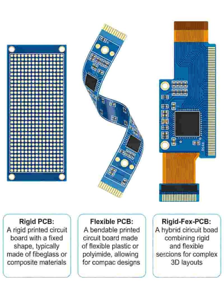
PCB Manufacturing Capabilities
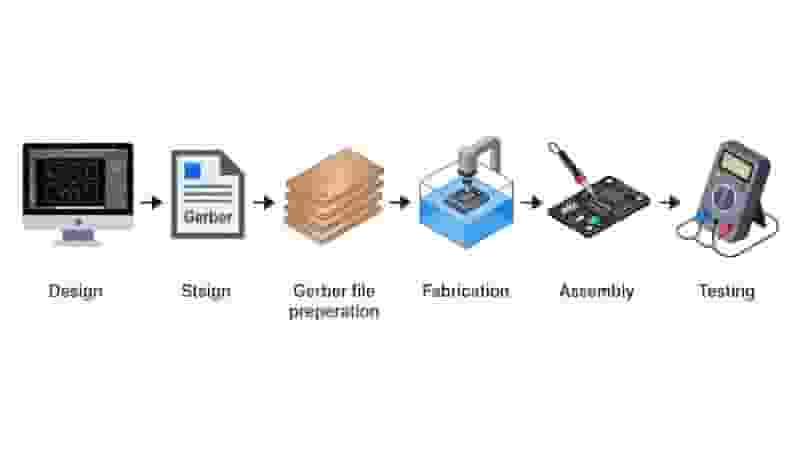
Learn the Essential Requirements for PCB Prototype Manufacturing in 2025
HASL: Hot Air Solder Leveling for PCB Surface Finish
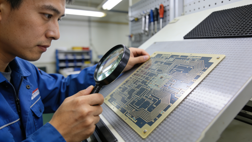
High-Precision PCB & SMT Stencil Manufacturing

Top Applications of Flexible Printed Circuit Boards in 2025