HDI PCB manufacturing provides high-density interconnect solutions with microvia, blind via, and buried via structures for compact, high-performance electronics. We deliver reliable HDI boards from prototype to mass production, supporting up to 30 layers for automotive, 5G, medical, and industrial applications.
What Is HDI PCB and Why Choose It
High-density interconnect (HDI) PCBs offer much higher wiring density than standard PCBs, using microvias, blind vias, buried vias, fine lines, and high-performance materials.
By shortening signal paths and optimizing routing, HDI PCBs create smaller, more reliable, and higher-speed electronic products for modern engineering demands.
- Pack more functions into a smaller footprint with microvia and via-in-pad
- Improve signal integrity and reduce high-speed noise
- Lower total system cost by reducing layer count
- Enhance reliability with optimized thermal and structural design
Microvia, Blind & Buried Via Structures
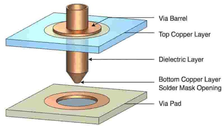
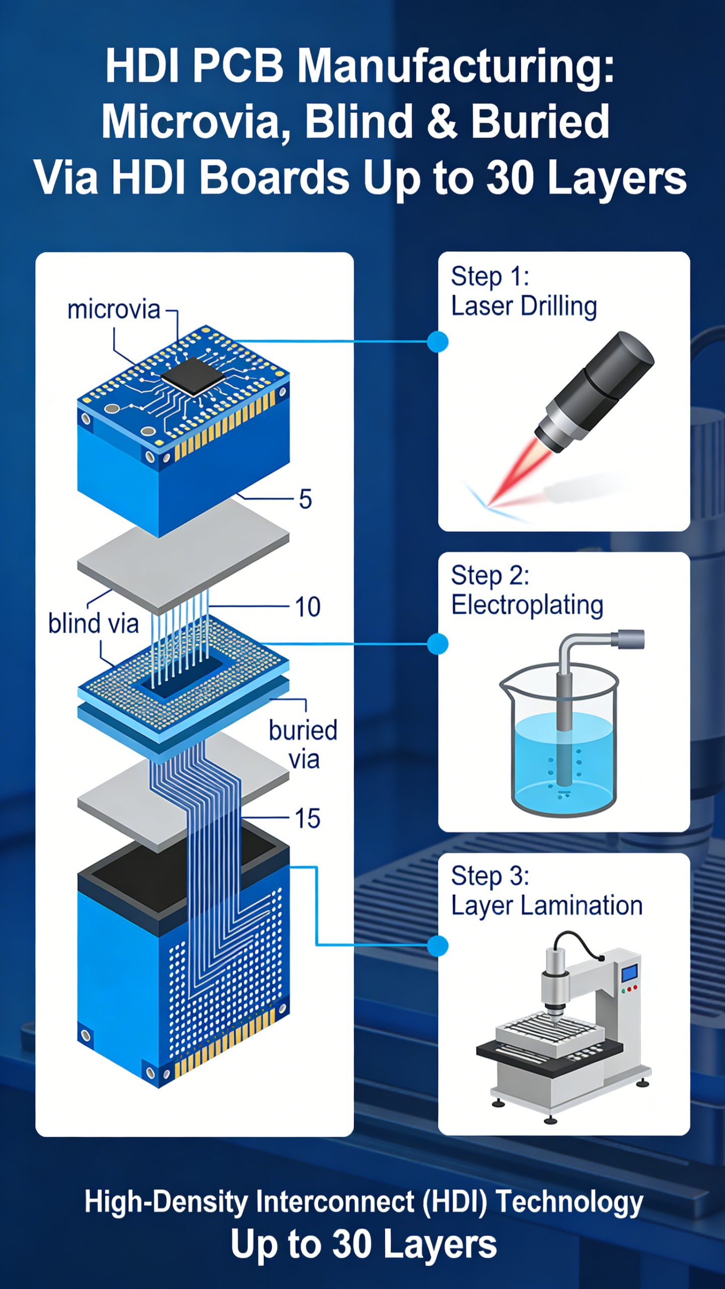
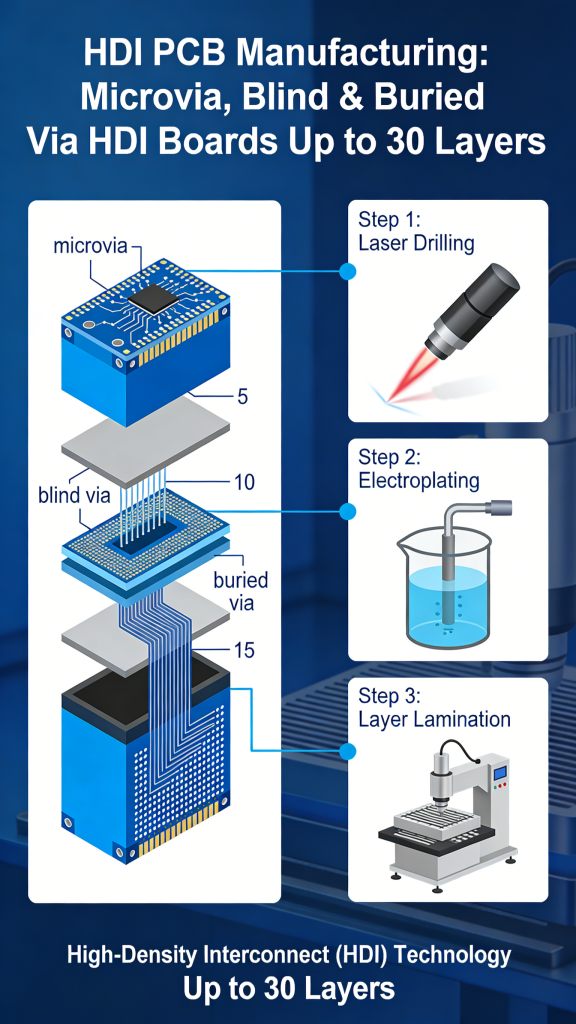
Our HDI PCB manufacturing uses precision laser drilling to build reliable via structures for high-density designs:
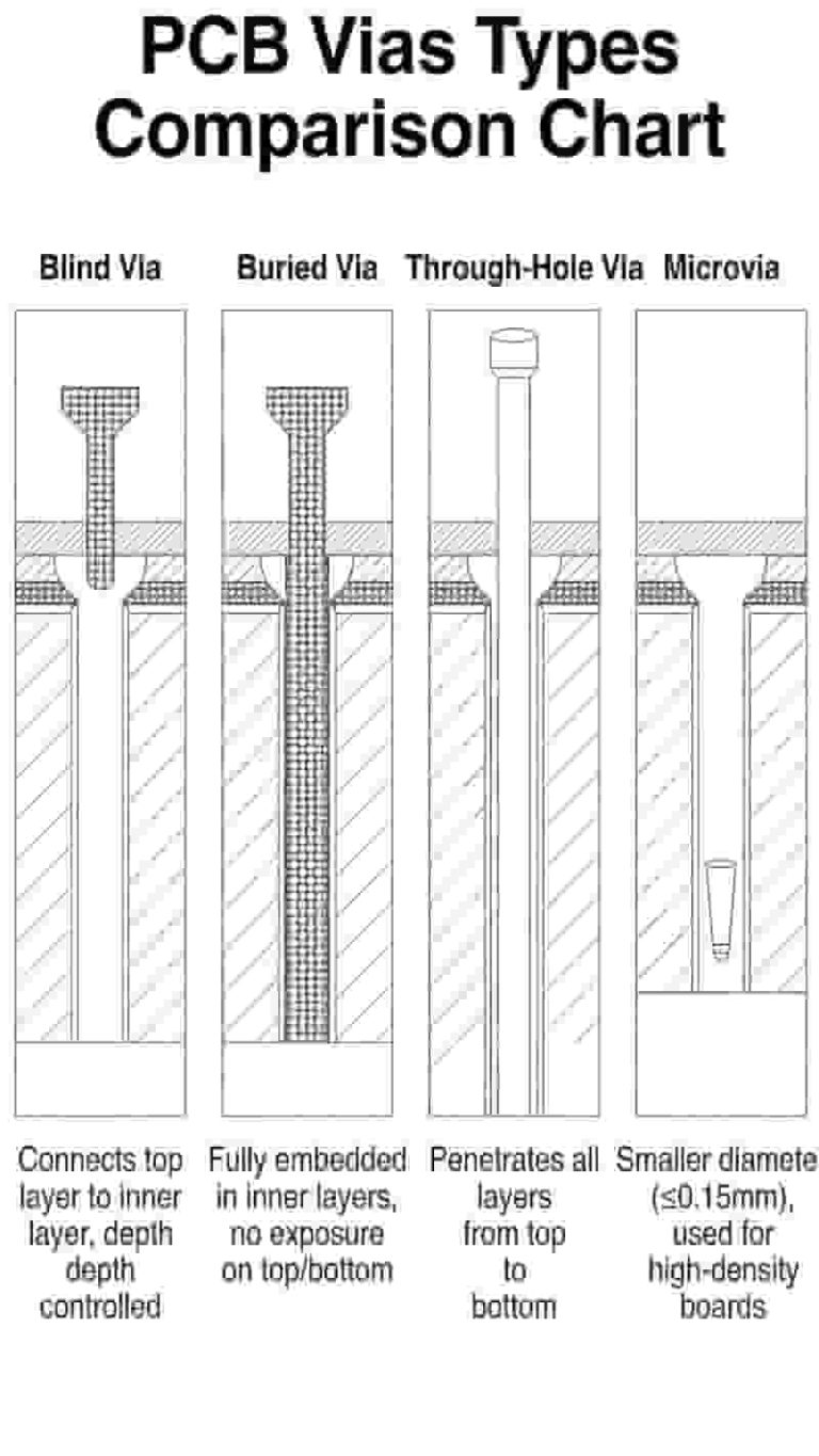
- Microvia: Laser-drilled vias down to 0.10 mm (4 mil)
- Blind Via: Connects outer layer to inner layer without full penetration
- Buried Via: Connects inner layers only, invisible on the surface
- Stacked & Staggered Vias: Advanced structures for maximum routing density
HDI PCB Manufacturing Capabilities
| Item | Specification |
|---|---|
| HDI Structure | 1+N+1, 2+N+2, 3+N+3, Any-Layer (ELIC) |
| Max Layers | Up to 30 Layers |
| Min Trace/Space | 3/3 mil (0.075 mm) |
| Min Microvia | 0.10 mm (4 mil) laser drilled |
| Materials | High-Tg, Low-loss, Halogen-free laminates |
| Surface Finish | ENIG, ENEPIG, Immersion Silver, HASL, Gold Fingers |
| Certificates | UL, ISO 9001, IATF 16949, RoHS |
HDI Stackup Options
1+N+1 HDI – Cost-Effective Standard
Best for medium-density designs with 0.5 mm BGA pitch. Ideal for consumer electronics and IoT devices.
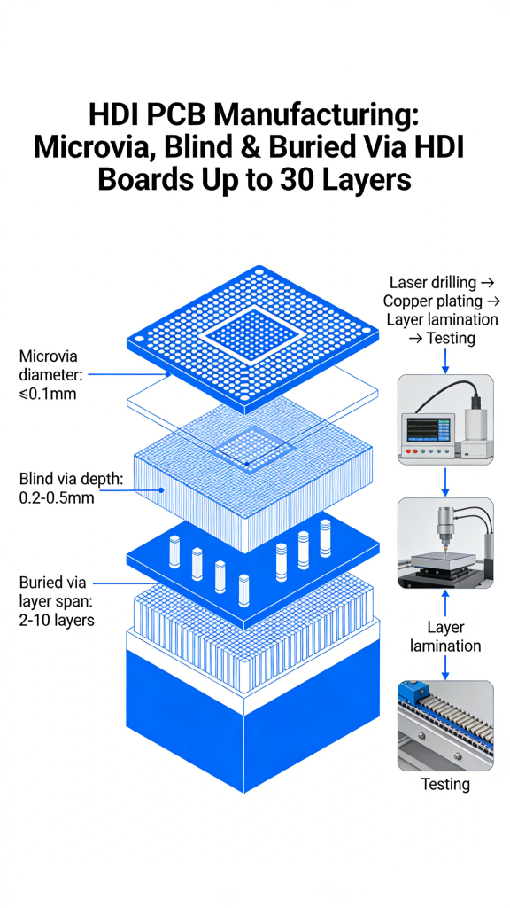
2+N+2 & 3+N+3 HDI – High-Density Performance2+N+2 & 3+N+3 HDI – 高密度性能
Designed for fine-pitch BGAs (0.4 mm and below) and high-speed circuits. Used in 5G, automotive, and high-end devices.
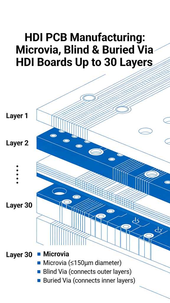
Any-Layer (ELIC) HDI – Ultimate Density
Maximum interconnect density for flagship products, allowing microvias between any layers.
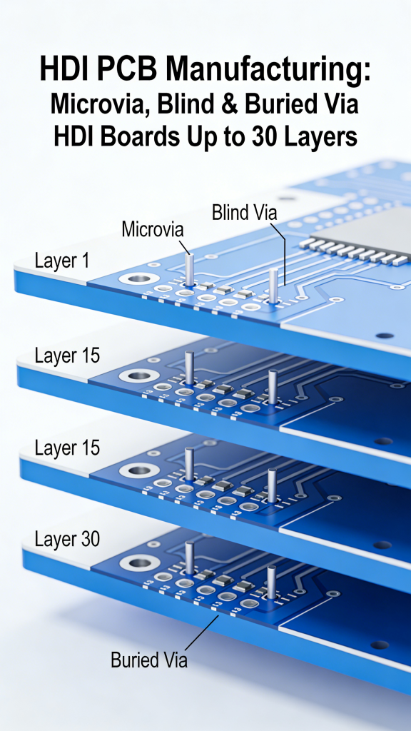
Quality & Reliability Control
Our HDI PCB manufacturing ensures consistent quality through strict process control:
- Precision laser drilling and sequential lamination
- AOI inspection for inner and outer layers
- X-ray inspection for microvia and buried via quality
- Full electrical testing for continuity and impedance
- Professional DFM review for all HDI PCB designs
HDI PCB Cost & Lead Time
The cost of HDI boards depends on stackup type, layer count, materials, and order quantity.
- Prototype Lead Time: 5–8 working days
- Production Lead Time: 10–15 working days
- Expedited service available for urgent projects
Industries & Applications
Our HDI PCBs serve high-reliability markets worldwide:
- Automotive & EV: ADAS, ECU, infotainment, power control
- 5G & Telecom: high-speed networking, base stations, modules
- Medical Devices: portable monitors, diagnostic equipment
- Consumer Electronics: smartphones, wearables, tablets
- Industrial & IoT: automation, robotics, sensors
Request HDI PCB Quote
Get professional HDI PCB manufacturing with fast quotes, reliable quality, and global delivery. No MOQ for prototypes, 24-hour engineering review and DFM support.
Get Your Free HDI PCB Quote Today
Upload Gerber & Get Quote
Summary
We are a trusted partner for professional HDI PCB manufacturing, providing high-quality HDI boards with microvia, blind via, and buried via technology up to 30 layers. With advanced production, strict quality control, and full engineering support, we deliver reliable HDI solutions for global industrial buyers.
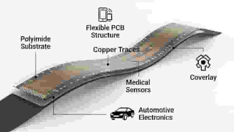
Flexible PCB Manufacturing Process Steps: Complete Technical Guide
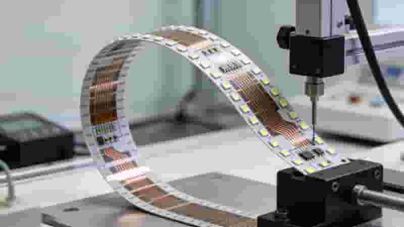
Professional LED PCB Manufacturing & Assembly Services
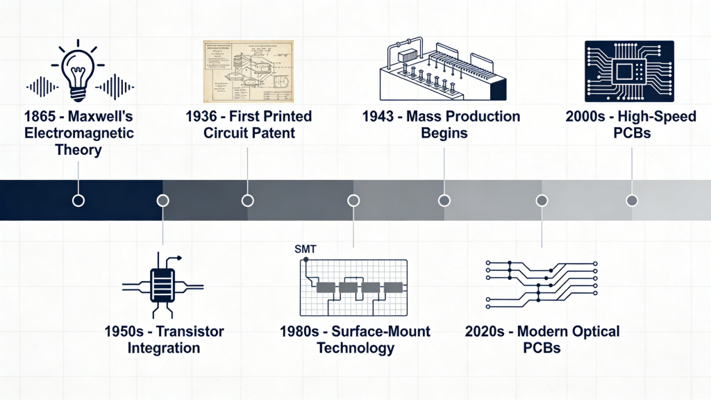
The Historical Timeline and Future Outlook of Printed Circuit Boards
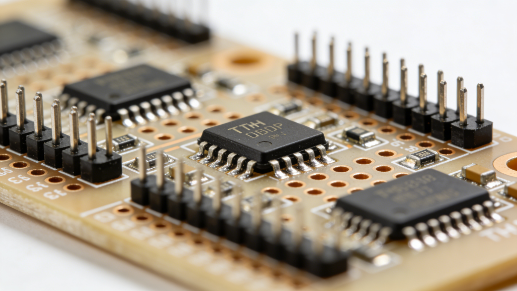
Demystifying THT PCB Assembly: A Comprehensive Professional Guide
Printed Circuit Board Assembly Services | Full Turnkey PCBA Solutions