PCB Solder Mask (also known as solder resist) is a protective polymer layer applied to printed circuit boards to prevent solder bridging, resist oxidation, improve insulation, and ensure long‑term reliability in SMT assembly and industrial applications. This guide covers definitions, types, colors, processes, DFM rules, IPC standards, testing, and troubleshooting for engineering and procurement teams worldwide.
What Is PCB Solder Mask?
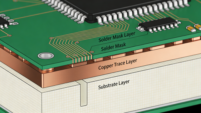
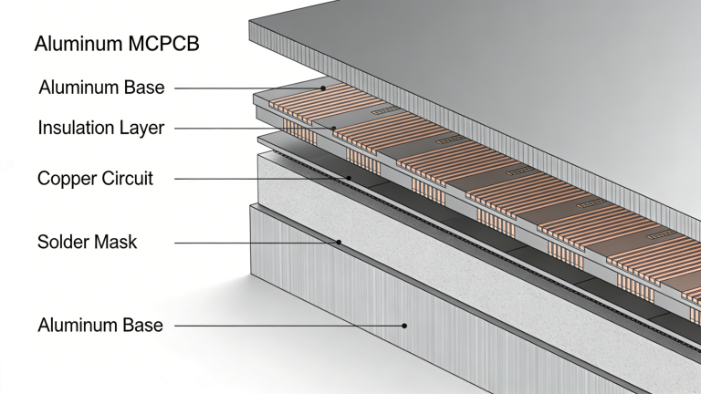
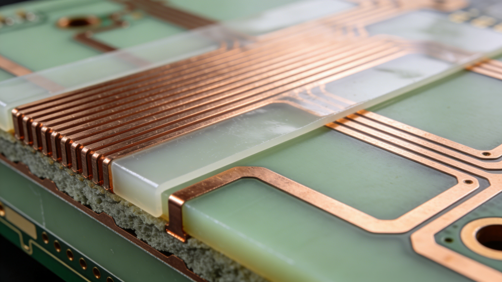
PCB Solder Mask is a permanent protective coating that covers most copper traces while exposing only component pads and test points. It is essential for PCB manufacturing, preventing short circuits, environmental corrosion, and assembly failures.
Without a qualified PCB Solder Mask, PCBs face high risks of solder bridging, oxidation, insulation failure, and shortened service life—directly increasing assembly costs and quality risks.
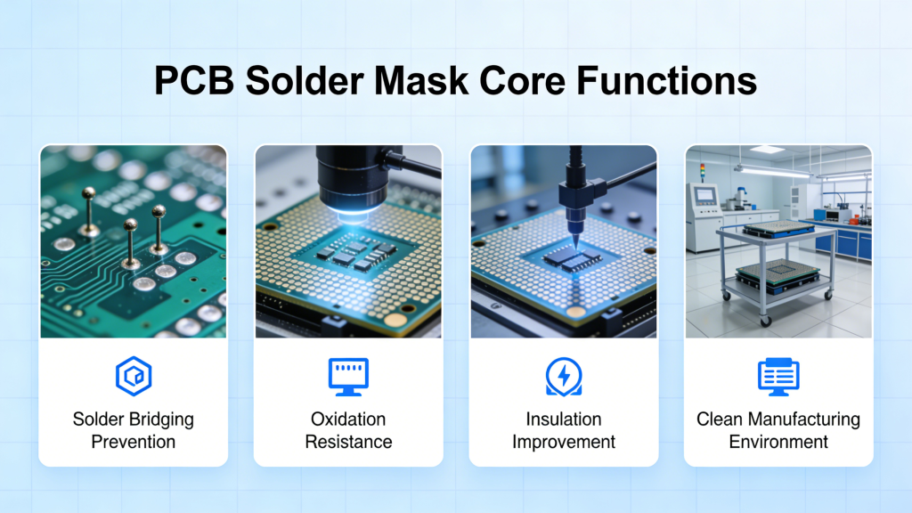
Core Functions of PCB Solder Mask
- Prevents solder bridging during reflow and wave soldering
- Protects copper from oxidation, humidity, chemicals, and abrasion
- Enhances electrical insulation and high‑voltage resistance
- Improves SMT assembly yield and reduces defects
- Provides stable performance under thermal shock and cycling
- Offers visual contrast for manual and AOI inspection
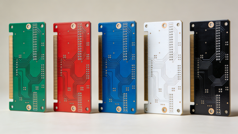
PCB Solder Mask Colors & Applications
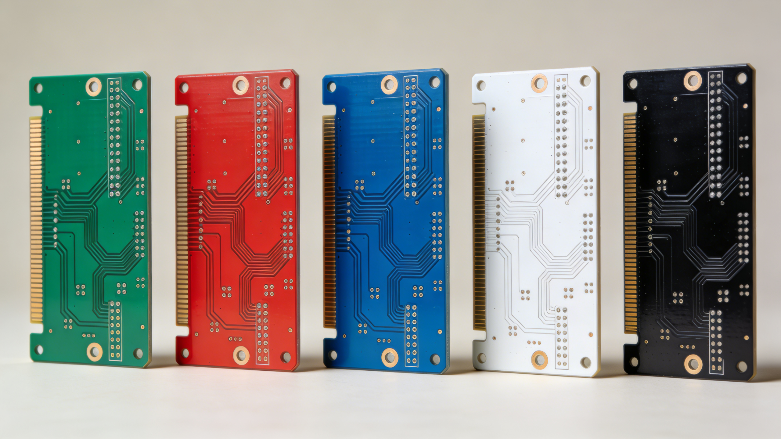
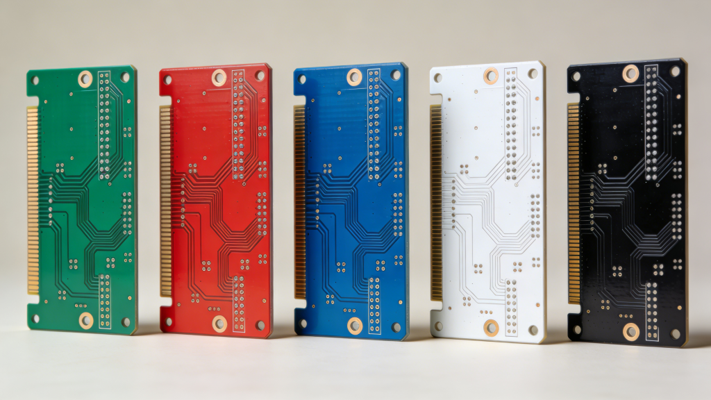
Color does not change core electrical performance, but affects inspection, lighting, and branding. The most widely used PCB Solder Mask colors include:
- Green: Industry standard; best for AOI and cost‑effective
- Red / Blue: High visibility for project differentiation
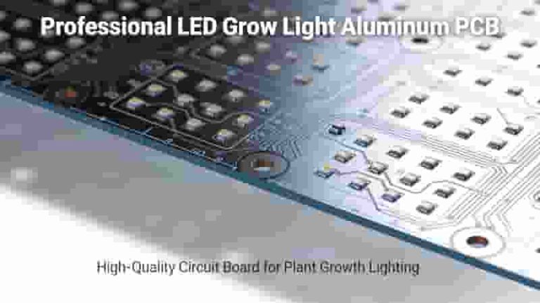
- White: Ideal for LED PCBs to improve light reflection
- Black: Anti‑glare for display and optical devices
- Matte Green / Black: Premium for anti‑reflective designs
4 Main Types of PCB Solder Mask
1. Liquid Photoimageable (LPI) Solder Mask
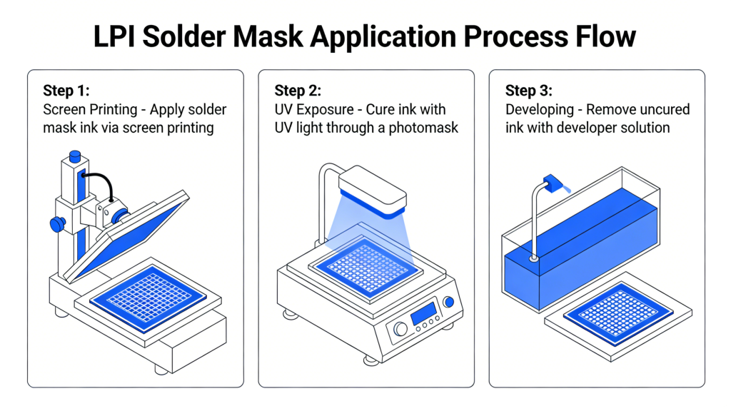
The most common PCB Solder Mask for industrial and high‑precision PCBs. Applied by screen printing, spraying, or curtain coating, then UV exposed and developed. Offers high resolution, strong adhesion, and stable performance.
2. Dry Film Photoimageable Solder Mask
Used for HDI and heavy‑copper PCBs. Laminated under vacuum for uniform thickness. Delivers ultra‑high precision but at a higher cost.
3. Epoxy Liquid Solder Mask
Low‑cost option for low‑density boards. Applied by screen printing without photolithography. Suitable for simple consumer electronics.
4. Peelable Solder Mask
Temporary protection for specific areas during surface finishing and assembly. Can be removed cleanly without residue.
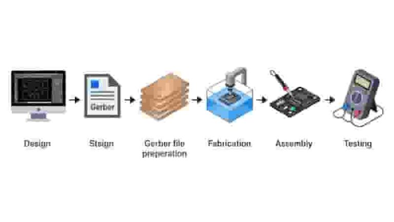
Full PCB Solder Mask Manufacturing Process
- Pretreatment: Cleaning and roughening copper surface
- Coating: Applying PCB Solder Mask ink
- Pre‑baking: Evaporating solvent
- Exposure: UV curing patterned areas
- Developing: Removing unexposed ink
- Final Curing: Enhancing hardness and adhesion
- Inspection: Checking defects per IPC standards
PCB Solder Mask Type Comparison Table
| Parameter | LPI Solder Mask | Dry Film | Epoxy Liquid |
|---|---|---|---|
| Precision | High | Ultra High | Low |
| Cost | Medium | High | Low |
| Application | General & High‑Precision | HDI & Heavy Copper | Simple Low‑Density |
IPC Standards & Quality Testing
All PCB Solder Mask production follows international standards:
- IPC‑SM‑840: Solder mask performance requirements
- IPC‑SM‑781: Application and design guidelines
- Adhesion Test: IPC‑TM‑650 2.4.28.1
- Hardness Test: Pencil hardness per JIS
- Heat Resistance: 260°C tin dipping test
- RoHS & REACH compliance for global export
Common Issues & Solutions
- Peeling: Improve pretreatment and curing parameters
- Uneven Coating: Optimize ink viscosity and application speed
- Bridge Breaking: Increase exposure energy and control thickness
- Color Difference: Standardize ink mixing and baking
- Misregistration: Stabilize temperature and film alignment
Summary
PCB Solder Mask is a critical layer for PCB reliability and assembly quality. Choosing the right type, color, and process ensures high yield, long service life, and compliance with global industry standards.
For industrial buyers and engineers, prioritizing IPC compliance, DFM optimization, and stable manufacturing processes is the key to successful PCB projects.
Need Professional PCB Solder Mask Solutions?
Get free DFM analysis, custom color options, IPC‑certified production, and fast global delivery. Contact us for a detailed quote today.
Request PCB Quote Now
How to Choose a Reliable PCB Manufacturer in Europe: Complete Guide for Industrial Buyers
Aluminum, Copper & Flexible LED Circuit Boards with Superior Heat Dissipation
PCB Classification Guide: Types, Applications & Selection for Beginners & Pros
PCB Vias: Complete Guide to Types, Design, Reliability and Performance
Ball Grid Array (BGA) PCB Manufacturing & Assembly Services