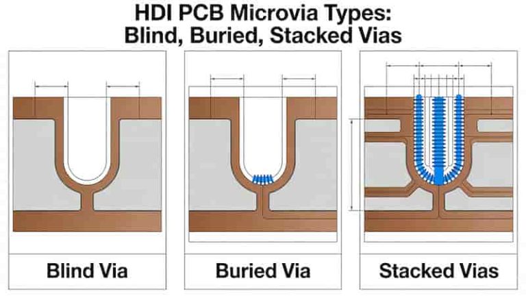
This guide covers core PCB pad design principles, component spacing, IPC standards, SMD/through-hole rules, thermal management, and DFM to boost assembly yield, reliability, and performance for industrial and export-grade PCBs.
PCB Component Layout & Spacing Rules
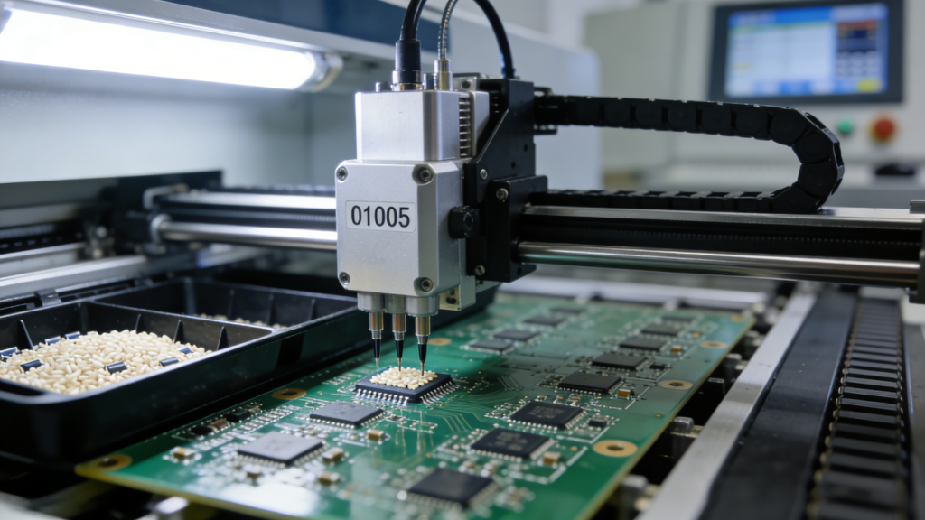
When laying out PCB components, designers must balance minimum component spacing against component height and thickness. Proper spacing prevents assembly interference, soldering defects, and thermal crowding.
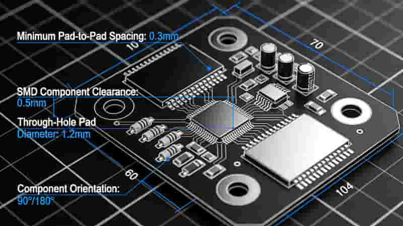
- Increase clearance between tall/large components to avoid shadowing thin components during reflow.
- Maintain consistent spacing to prevent solder bridging, cold joints, or component damage.
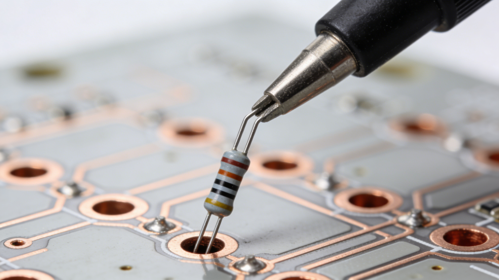
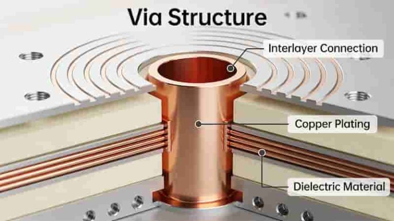
- Components are mechanically secured and electrically connected via PCB pad design and plated through holes.
- Poor soldering practices can lift or damage pads, leading to full board failure.
What Are PCB Pads?
A PCB pad consists of a plated through hole or surface mount area and its surrounding copper foil. It is the fundamental conductive unit that forms electrical connections and mechanical bonds for components.
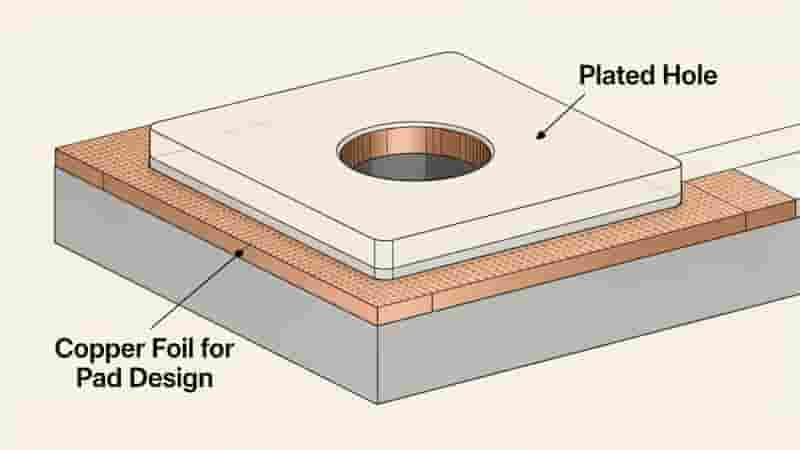
A complete land pattern is a group of pads tailored to a specific component package, enabling reliable SMT or through-hole assembly.
Common PCB Pad Shapes & Uses
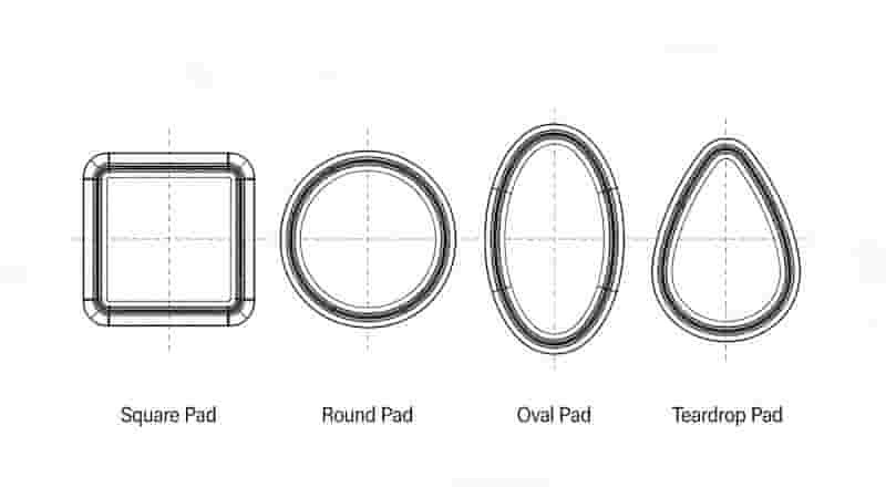
Different pad shapes support various assembly methods, board densities, and manual or automated production.
| Pad Shape | Main Application & Features |
|---|---|
| Square Pads | Large boards with few components, easy for manual fabrication |
| Round Pads | Single/double-sided PCBs, strong bonding performance |
| Oblong/Oval Pads | Dense layout design, space-saving with reliable solder joints |
| Specialty Pads | Diamond, plum, teardrop: for high-stress, large-aperture and thermal scenarios |
Critical PCB Pad Design Standards
Standardized PCB pad design ensures manufacturability, reliability, and compatibility with global assembly lines.
| Specification | Standard Requirement |
|---|---|
| Minimum width of single-sided PCB pad | ≥ 0.25 mm |
| Maximum pad diameter | ≤ 3 × component hole diameter |
| Minimum diameter of single-sided PCB pad | 1.6 mm |
| Double-sided low-current pad | Hole diameter + 0.5 mm |
| Hole > 1.2 mm / Pad diameter > 3.0 mm | Adopt diamond / plum shape pads |
| Auto-insert components | Teardrop pads along leg bend direction for full solder coverage |
| Large copper areas | Use thermal relief (chrysanthemum) pads to prevent cold joints |
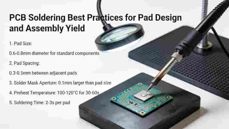
Soldering Best Practices for Pad Protection
Improper soldering is a leading cause of pad liftoff and board scrap. Follow these rules to protect PCB pad design integrity.
| Category | Key Rules & Notes |
|---|---|
| Soldering Iron Temperature | Avoid excessive temperature to prevent copper separation |
| Pad Size Selection | Do not use over-sized pads to avoid solder bridging |
| Large Copper Planes | Apply thermal relief pads |
| Manual Soldering | Control heat and dwell time to protect pad adhesion |
Summary
Correct PCB pad design and component spacing are essential for high-yield assembly and long-term reliability. Following industry standards for pad size, shape, and soldering practices minimizes defects and supports consistent production for global industrial applications.
Need Professional PCB Manufacturing & Assembly?
We provide DFM analysis, optimized PCB pad design, prototyping, and mass production for global buyers. Get a fast, precise quote today.