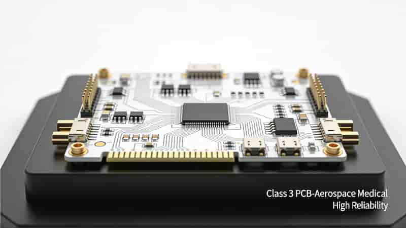
This professional guide covers flexible PCB materials, fabrication, SMT assembly, quality control, and best practices for engineers, buyers, and global importers. Learn how to ensure reliability, consistency, and cost efficiency for your flex PCB projects.
Why Choose Flexible PCBs?
Flexible PCB devices offer distinct advantages over rigid PCBs, making them ideal for modern electronics with dynamic shape requirements:
- Lightweight & Compact: Thinner construction saves space and reduces weight for portable devices.
- Dynamic Flexibility: Bend radii as low as 0.1 mm enable electronics to fit irregular shapes.
- High-Density Interconnects: Fine trace/space (25/25 μm) supports complex circuits in tight spaces.
- Enhanced Signal Integrity: Stable high-frequency performance at bends ensures reliable transmission.
- Superior Heat Dissipation: Copper heat-spreader layers optimize thermal management.
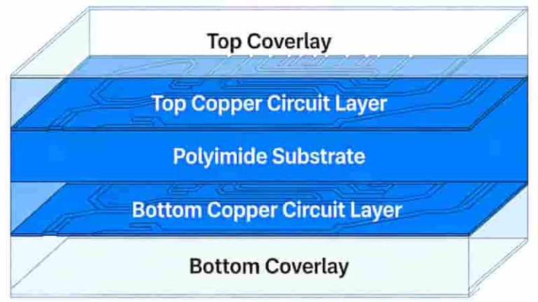
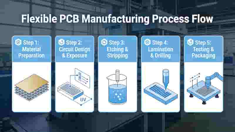
Flexible PCB Fabrication Process
Flexible PCB manufacturing uses specialized materials and precision processes to ensure durability and performance.
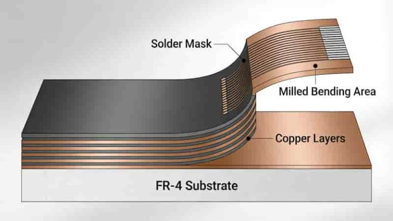
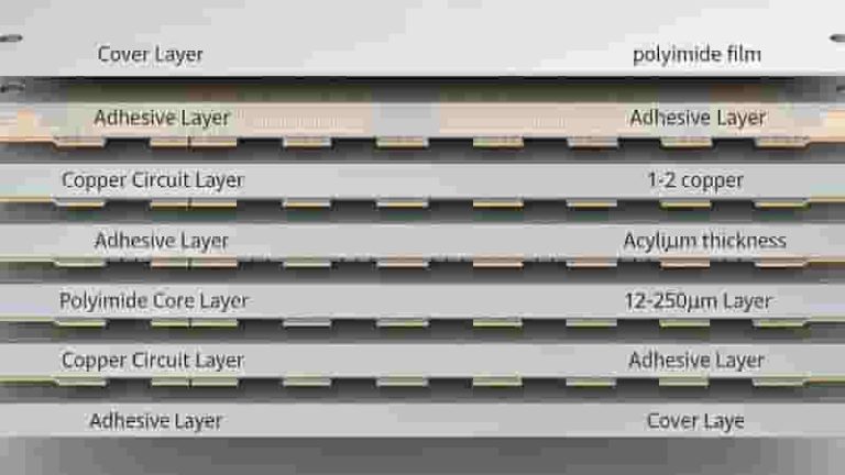
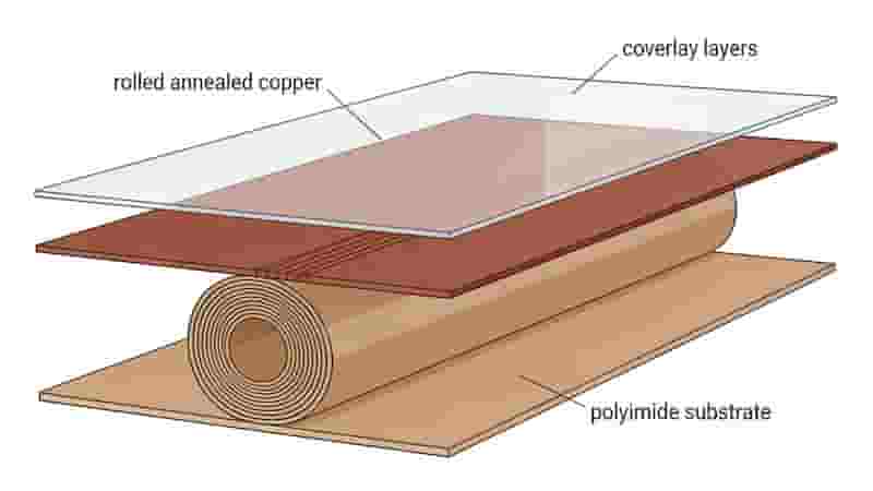
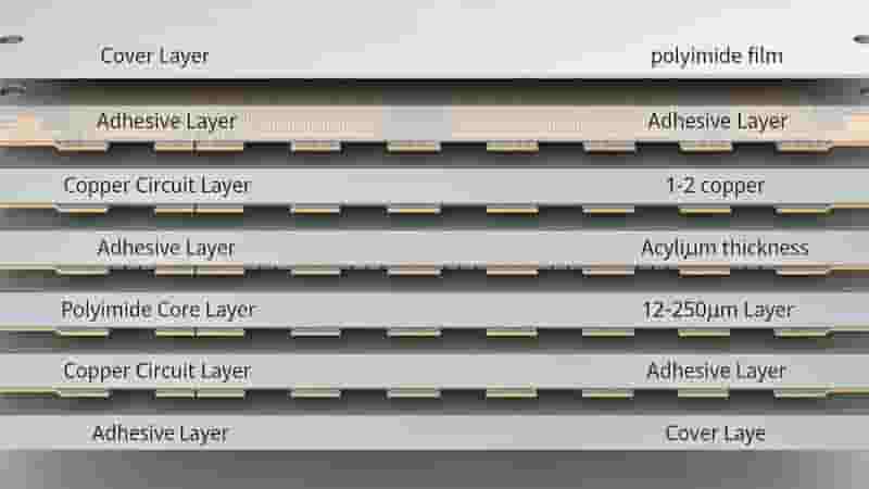
Materials
Polyimide (Kapton) is the primary substrate for heat resistance and flexibility. PET films are used for cost-sensitive projects. Circuit layers use rolled annealed copper etched via photolithography.
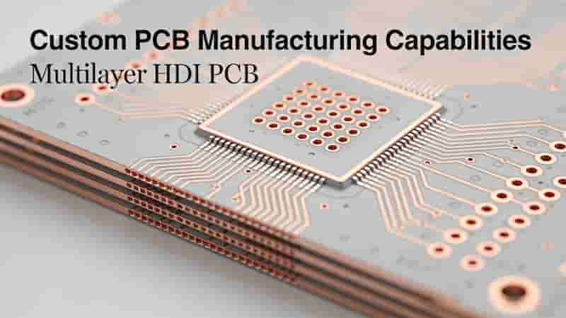
Our Capabilities
- Multilayer flex PCB (2–12 layers) with adhesive dielectric films
- Plated-through holes and microvias down to 50 μm
- AOI and electrical testing for full quality assurance
Key Flexible PCB Design Considerations
Designing reliable flex circuits requires strict attention to these factors:
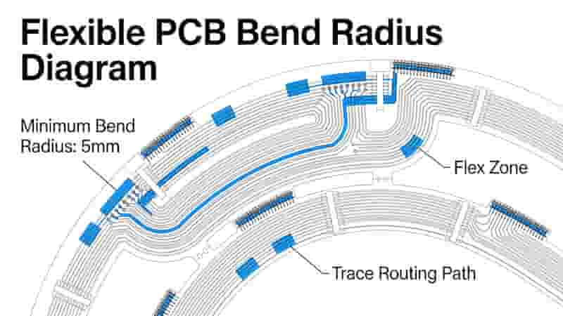
- Bend Radius: Optimize stackup to reach 0.1 mm for long-term durability
- Board Stiffness: Use selective stiffeners to balance flex and rigidity
- Thermal Management: Copper planes with thermal reliefs prevent stress
- High-Frequency Layout: Controlled impedance for RF and digital stability
- Component Selection: Low-profile SMT components resist flex fatigue
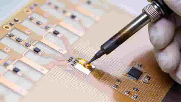
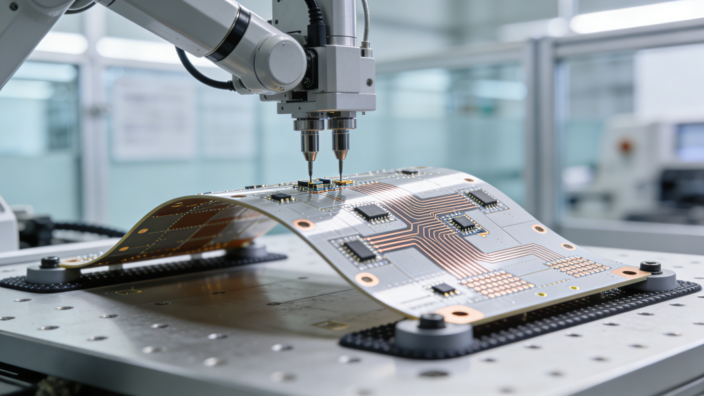
Advanced Flex PCB Assembly Techniques
Flex PCB assembly demands precision to protect delicate polyimide substrates.
Assembly Methods
- SMT Assembly: Pick-and-place + reflow soldering for high efficiency
- Manual Assembly: For complex high-density layouts
- Attachment: Solder, conductive epoxy, or mechanical fasteners
Rework & Repair
Specialized equipment safely replaces components without damaging flex layers.
Applications & Future Trends
Flexible PCB technology powers innovation across industries:
- Wearable devices & health trackers
- IoT sensors & smart home electronics
- Automotive interior & movable systems
- Medical implants & diagnostic tools
- Robotics, UAVs & foldable electronics
By 2026, flex circuits will lead 6G antenna, flexible display, and sustainable manufacturing trends.
Summary
This guide covers the full lifecycle of flexible PCB manufacturing and assembly, from materials and design to production and applications. With professional processes, strict quality control, and engineering support, we deliver reliable flex circuits for global industrial buyers.
Get Your Flexible PCB Solution
We provide professional flexible PCB manufacturing and turnkey assembly services for global importers, engineers, and procurement teams. We offer free design reviews, fast prototyping, competitive pricing, and reliable mass production.
Contact us today for a free quote, custom solution, or technical consultation!
IPC Standards: Complete Guide for PCB Manufacturing & Assembly
PCB Solder Mask: The Complete Technical Guide for Global Buyers

Top 30 Best Free PCB Design Software Free Download
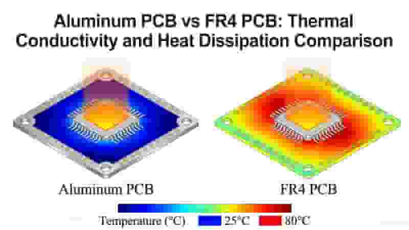
Aluminum PCB vs FR4 PCB: Full Technical Comparison for Industrial & High-Power Applications
Types of Flexible Circuit Boards: The Ultimate Guide to Flex PCBs