Semi-Flex PCBs deliver the ideal balance of rigidity and flexibility for modern electronics. Built on standard FR-4 with precision thinned bending zones, they offer cost efficiency, reliable performance, and easy assembly, filling the critical gap between traditional rigid PCBs and high-cost flex circuits. Ideal for static bend installations, Semi-Flex PCBs reduce assembly complexity while enhancing product durability and design freedom.
What Are Semi-Flex PCBs
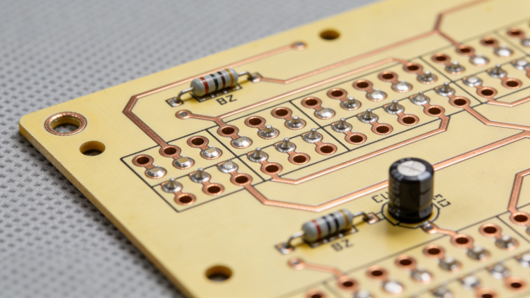
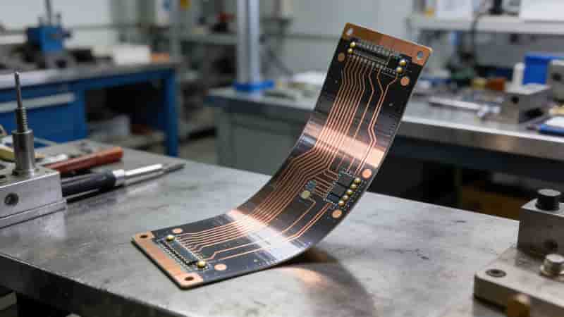
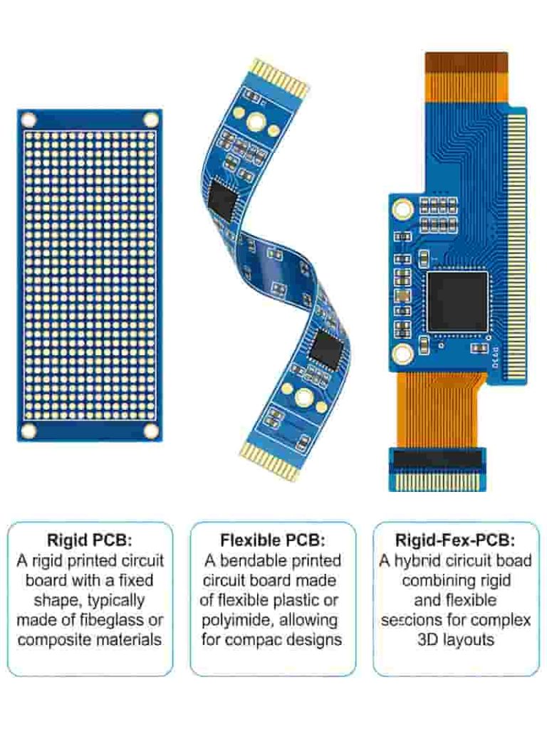
Printed circuit boards form the backbone of all electronic devices. Rigid PCBs offer stability but no flexibility, while flex PCBs bend freely but lack structural strength. Semi-Flex PCBs solve this dilemma by combining both properties in one board.
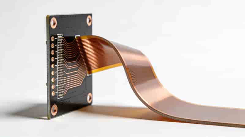
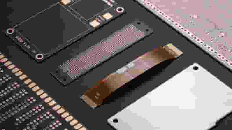
Semi-Flex PCBs are rigid PCB derivatives with selectively milled thin zones (0.10mm to 0.30mm) that allow controlled static bending. They are designed for one-time flex-to-install use, not repeated dynamic flexing, making them perfect for compact enclosures in automotive, telecom, and consumer electronics.
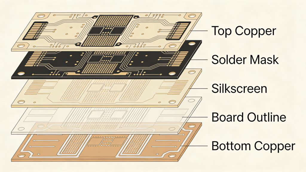
Materials & Structure of Semi-Flex PCBs
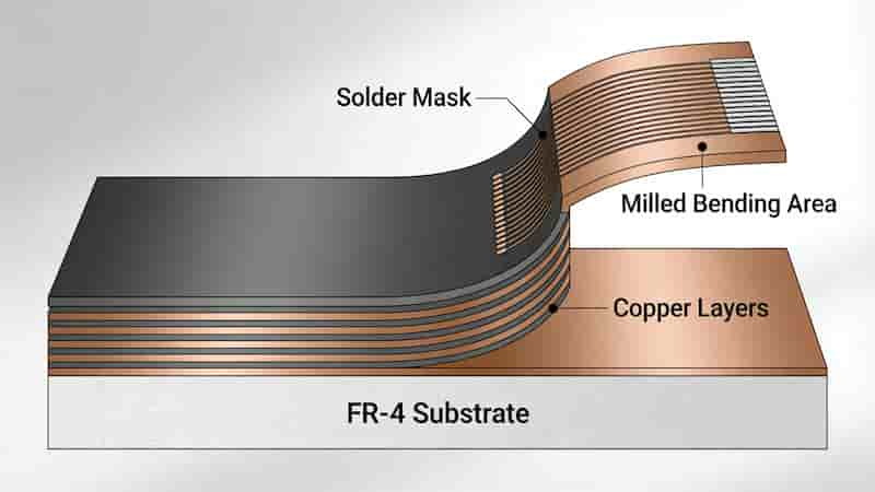
Semi-Flex PCBs use industry-standard FR-4 material as the core substrate, the same reliable material used in most rigid PCBs. No expensive polyimide flex layers are required, keeping costs low.
Key structural features:
- Bending zones milled to 0.10 to 0.30mm thickness
- 2 to 8 conductive copper layers (35μm standard)
- Standard solder mask (green/black/blue)
- PTH vias, buried vias for layer connectivity
- Surface finishes: ENIG, Immersion Tin, OSP
Key Advantages of Semi-Flex PCBs
1. Cost Efficiency: 30% to 50% lower than rigid-flex PCBs by using FR-4 instead of polyimide
2. High Reliability: FR-4 rigid sections match standard PCB durability
3. Design Freedom: 3D routing fits tight spaces without connectors
4. Easy Assembly: Compatible with standard SMT assembly lines
5. Shorter Lead Time: Uses rigid PCB manufacturing processes
6. Space & Weight Saving: Eliminates cables and connectors for compact designs
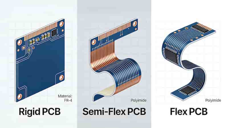
Comparison: Rigid vs Semi-Flex vs Flex vs Rigid-Flex PCBs
| Parameter | Rigid PCB | Semi-Flex PCB | Flex PCB | Rigid-Flex PCB |
|---|---|---|---|---|
| Material | FR-4 | FR-4 (thinned) | Polyimide | FR-4 + PI |
| Bending Type | None | Static one-time | Dynamic repeated | Static + dynamic |
| Cost | Lowest | Medium | High | Highest |
| Layers | 1 to 30+ | 2 to 8 | 1 to 6 | 2 to 12 |
| Best For | Standard devices | Static bend installs | Dynamic flex | High-end complex |
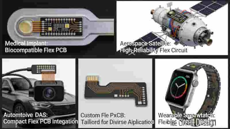
Industry Applications of Semi-Flex PCBs
Semi-Flex PCBs serve diverse industries where moderate bending and high reliability are required:
- Automotive: EV batteries, sensors, navigation systems, in-car controls
- Consumer Electronics: Wearables, laptops, smartphones, compact devices
- Industrial: Robots, control modules, sensors, test equipment
- Medical: Monitoring devices, imaging equipment, portable diagnostics
- Telecom: Routers, transceivers, compact communication hardware
- Aerospace: Avionics, guidance systems, lightweight electronics
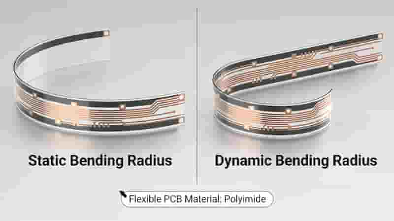
Design & Bending Guidelines for Semi-Flex PCBs
To ensure reliable performance of Semi-Flex PCBs, follow these critical design rules:
- Bend only with copper on the outside of the curve
- Minimum bending radius: 3 to 5x the board thickness
- Keep traces perpendicular to bending lines
- Avoid components and vias in bending zones
- Use 0.10 to 0.30mm thickness for flex areas
- Limit bending to one-time installation only
Our Semi-Flex PCB Manufacturing Capabilities
We specialize in high-quality Semi-Flex PCB manufacturing and assembly for global buyers. Our advanced facilities ensure precision, reliability, and cost efficiency:
- Layer count: 2 to 8 layers for Semi-Flex PCBs
- Minimum line width/space: 4/4mil (0.10mm)
- Minimum via size: 0.15mm
- Bending zone thickness: 0.10 to 0.30mm
- Full SMT assembly & testing services
- UL, RoHS, and IPC Class 2/3 compliance
Our engineering team provides free DFM analysis to optimize your Semi-Flex PCB design for manufacturability, performance, and cost.
Conclusion
Semi-Flex PCBs represent the optimal middle ground between rigid and flex circuit boards. They deliver the stability of FR-4 rigid PCBs with controlled flexibility for static installations, all at a lower cost than rigid-flex alternatives.
With broad industry applications, easy assembly, and excellent reliability, Semi-Flex PCBs are the smart choice for compact, high-performance electronic designs that need both rigidity and controlled bending.
Get Your Semi-Flex PCB Quote Today
Contact us for custom Semi-Flex PCB design, manufacturing, and assembly services. We provide fast quotes, DFM support, and high-quality production for global buyers.
Request a Quote
Contact Engineering
Single-Sided Flexible PCB Design Guide: Bending Radius, Trace Routing and Stiffeners
Gold Plating vs. Immersion Gold: What PCB Buyers Need to Know
Fast Turnaround PCB Prototype Services from Certified Manufacturer
Turnkey PCB Manufacturing and Assembly: Full One-Stop Solution Advantages
PCB Manufacturing Capabilities