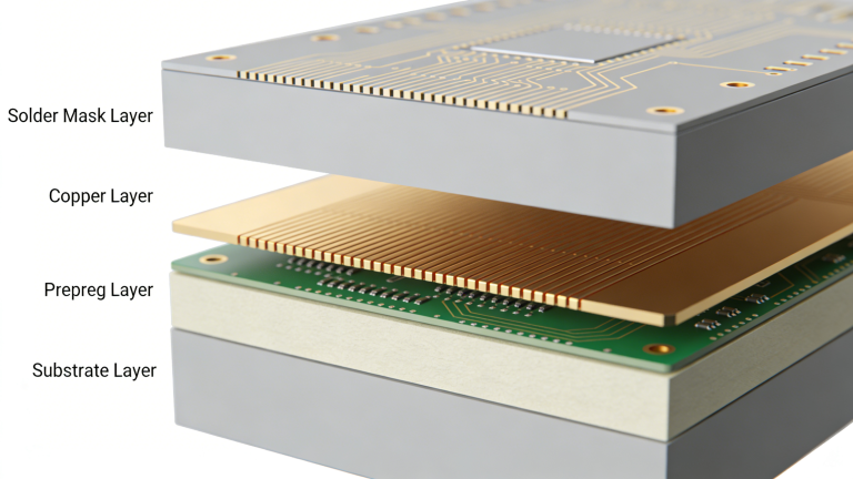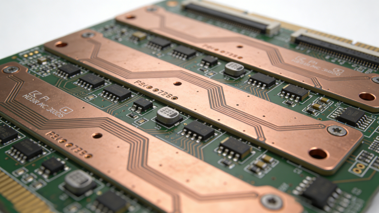
A 6 Layer PCB Board comprises three dielectric layers (insulating layers) and three conductive layers. The dielectric layers are usually made of fiberglass (a common material in PCB manufacturing) or other high-performance insulating materials, which provide electrical insulation between layers. Meanwhile, the conductive layers are typically composed of copper foil—with common thicknesses ranging from 0.5oz to 2oz—to enable efficient signal transmission and current conduction.
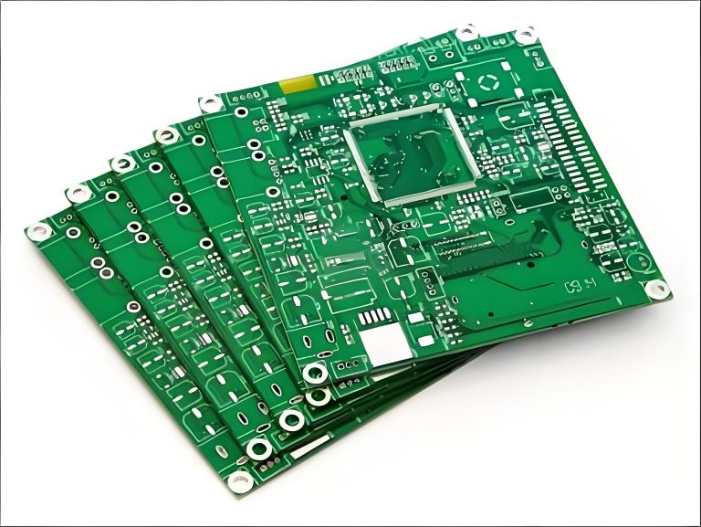
What is a 6 Layer PCB Board?
A 6 Layer PCB Board is a type of multilayer printed circuit board (MLB), similar to the4 Layer PCB Board but with enhanced functionality. Compared to a standard 4 Layer PCB, it adds two extra conductive layers—making it ideal for devices that need more wiring space without increasing board size.
A typical 1.6mm 6 Layer PCB Board stackup follows this structure (from top to bottom): Top Copper Layer (signal layer) → Prepreg (insulating layer) → Inner Copper Layer (power layer) → Core (insulating layer) → Inner Copper Layer (ground layer) → Prepreg (insulating layer) → Bottom Copper Layer (signal layer). This stackup design significantly improves EMI (Electromagnetic Interference) performance by separating power, ground, and signal layers—reducing signal interference in complex electronic devices.
6 Layer PCB Stackup Applications
6 Layer PCB Stackup works for many industries, thanks to its more wiring space and stable performance.
1. Consumer Electronics
Used in high-end products: 5G phones, smartwatches, high-end microwaves.
Why choose: Makes devices smaller, supports fast data transfer.
2. Telecommunications
Fits equipment like 5G base stations, GPS, satellite devices.
Why choose: Reduces signal interference, keeps transmission stable.
3. Medical Devices
Used for X-ray machines, CT scanners, heart monitors.
Why choose: Meets medical standards, works reliably 24/7.
4. Industrial Control
Suitable for PLC panels, robot controls, industrial sensors.
Why choose: Withstands extreme temps (-40℃~125℃) and vibration.
Standard and Typical 6 Layer PCB Stackup
PCB stackup is made of copper layers, core boards and PP layers. Even 6-layer PCBs (with at least 3 conductive layers) can meet different needs—layers connect via holes.
1. What’s Standard 6 Layer PCB Stackup?
Refers to the fixed layered structure of 6-layer PCBs, usually including 3 copper (conductive) layers + 3 insulation (core/PP) layers, suitable for most common scenarios.
2. Benefits of PCB Stackup
- Boosts function: Makes 6-layer PCBs transmit signals faster, supporting more powerful device functions.
- Improves durability: Protects inner layers from external damage, lasting longer.
- Reduces radiation: Minimizes equipment radiation (critical for high-frequency 6-layer PCBs); avoids extra EMI from bad impedance.
- Cuts costs: Puts multiple circuits on one 6-layer PCB, lowering manufacturing fees.
- Lessens crosstalk: Fixes poor impedance and signal interference issues.
The standard 6-layer PCB stackup works for most cases, but it’s not always the best fit. Below is a comparison of 3 other common stackup methods.
What is the Best 6 Layer PCB Stackup?
The “best” varies by needs. Below is a set of typical 6-layer PCB stackups for reference.
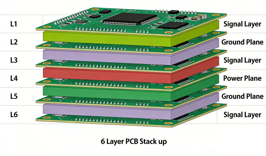
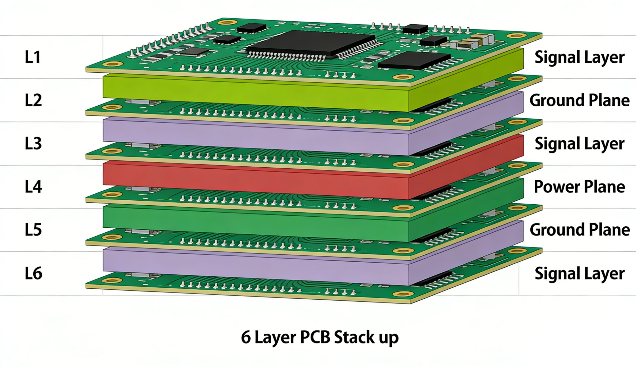
The structure is:
- Signal Layer
- Ground Plane
- Signal Layer
- Power Plane
- Ground Plane
- Signal Layer
This may not be your most satisfactory 6-layer PCB stack structure. The reason is that the signal layers in the circuit board have no shielding, and two of these signal layers are not adjacent to any ground plane. As signal integrity and performance grow increasingly important, this type of 6-layer PCB stack structure has been gradually abandoned.
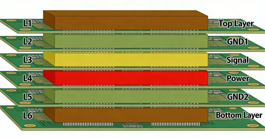
In this 6-layer PCB stack-up, the number of signal layers is reduced to 3 to add an extra ground layer. The structure is as follows:
- Top Signal Layer
- GND1
- Inner Signal Layer
- Power Plane
- GND2
- Bottom Signal Layer
This 6-layer PCB stack-up places each signal layer close to a ground plane, which helps achieve optimal return path performance. Additionally, placing the power plane and ground planes adjacent to each other creates planar capacitance. However, this design has a drawback: you will indeed lose one signal layer for routing.
6 Layer PCB Design Tutorial and Design Software
A proper stackup has a huge impact on 6-layer PCB design. Luckily, current PCB design software is powerful enough to let you fully create the stackup you need.
How to choose the right PCB design software? We’ve listed 30 free options for you to download.
On the right is a video tutorial for 6-layer PCB design using OrCAD—hope it helps you.
Learn more about 4 Solutions to Reduce EMC in 6-Layer PCB Design.
Quick Turn 6 Layer PCB Board Manufacturing
Compared with double-sided and 4-layer PCBs, 6-layer PCBs feature more layers and offer better routing performance. However, their fabrication cost and production difficulty are also higher.
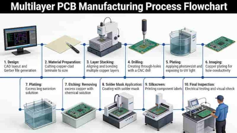
A 6-layer PCB is constructed by laminating layers onto a PCB core. After circuits are etched on the PCB core to form the third and fourth layers, the second and fifth layers are laminated under high temperature and pressure. Circuits are then etched on these two layers. The top and bottom layers are further laminated onto the 4-layer board, followed by circuit etching. Solder mask is applied to the top and bottom layers, and surface finish is processed on the PCB pads.
There are two types of PCB layer circuit etching methods:
- Positive plane etching
- Negative plane etching
With the continuous development of SMT (Surface Mount Technology) and the launch of new-generation SMD (Surface Mount Devices) such as QFP, QFN, CSP, and BGA (especially MBGA), electronic products have become more intelligent and miniaturized. This has driven major reforms and advancements in PCB industrial technology.
Accordingly, the progress of PCB manufacturing technology has also made 6-layer PCB production easier.
Materials for 6-layer PCB manufacturing
Printed circuit boards must be flame-resistant; they should only soften at a specific temperature rather than burn. This temperature is known as the glass transition temperature (Tg point), and this value is related to the dimensional stability of the PCB.
Standard PCB materials have a Tg value above 130°C, medium Tg materials are approximately 150°C, and high Tg materials are generally above 170°C.
Typically, PCBs with a Tg value ≥ 170°C are referred to as high Tg PCBs.
Multilayer circuit boards such as 6-layer PCBs generally adopt high Tg materials in production.
Normal Tg material (Tg 130–135°C) & High Tg material (above 170°C)
| Normal Tg material (Tg 130–135°C) | High Tg material (above 170°C) | ||
|---|---|---|---|
| Manufacturer/Brand | Material | Manufacturer/Brand | Material |
| ShengYi | S1141 | ShengYi | S1000-2 |
| S1155 | S1141 | ||
| NanYa | NP-140TL | S1170 | |
| KingBoard | KB-6160 | S1165 | |
| ISOLA | FR406/FR408 | ||
| ARLON | High Tg210 11N | ||
| GETEK | High Tg180 ML200/RG200 | ||
| NELCO | High Tg175 N4000-6/N4000-11 | ||
| High Tg190 N4000-12 | |||
| High Tg210 N4000-13 | |||
| ITEQ | IT180 |
High-frequency material (RF boards)
| Manufacturer/Brand | Material |
|---|---|
| Rogers | RO4000 Series |
| RT5000/RT6000 Series | |
| Taconic | TLX Series |
| Orcer | RF-35/RF-60 Series |
Prepreg Material Information
| Manufacturer/Brand | Material |
|---|---|
| KingBoard | KB-6050 Prepreg |
| KB-606X |
Prepreg Type
| Prepreg Type | Thickness (mm) | Resin Content | Dielectric Constant |
|---|---|---|---|
| 2116 | 0.12 | 55% | 4.5 |
| 7630 | 0.2 | 55% | 4.7 |
| 7628 | 0.185 | 43% | 4.7 |
| 1080 | 0.075 | 65% | 4.2 |
How to choose the best 6-Layer PCB manufacturer?
Choosing a capable 6-layer PCB manufacturer is critical to realizing your PCB design concept. A good multilayer PCB manufacturer must be efficient and reliable. Here are the factors to consider when selecting a 6-layer PCB manufacturer:
Rich experience: PCB manufacturing experience determines whether a manufacturer can successfully fulfill your 6-layer PCB order. Therefore, it is crucial to choose a reliable manufacturer with long-term experience in 6-layer PCB production.
Certification and licensing: Top 6-layer PCB manufacturers must hold valid qualifications, and their products should comply with IPC standards for the PCB industry.
Quick Turnaround Time: Turnaround time refers to the period required to complete an order. You will want your manufacturer to deliver high-quality boards within an agreed lead time.
Technical support: Strong PCB manufacturers can assist with your PCB design and provide technical support including DFM, DFT, and DFA.
Customer Service: You will want your PCB manufacturer to understand and satisfy your requirements. You should choose a manufacturer that responds promptly to customer needs and complaints.
JHY is a reliable and trustworthy PCB manufacturer and supplier based in China. Founded in 2011, we specialize in manufacturing single-sided, double-sided, and multilayer rigid PCBs, flexible PCBs, rigid-flex PCBs, HDI PCBs, as well as prototype and high-volume PCB production. We can fabricate and assemble PCBs from 1 to 64 layers.
6 Layer PCB Prototype Price
As a professional multilayer PCB manufacturer in China, we offer competitive and reasonable pricing for clients. We provide low-cost, high-quality 6-layer PCB prototype manufacturing services with fast turnaround times.
6-layer PCB prototype fabrication helps you quickly verify your stackup and design, detect errors and defects in a timely manner, and reduce unnecessary losses before mass production.
Standard delivery for 6-layer PCB prototypes takes 5-7 days, while express prototyping is available within 72 hours.
You can get a quick, free quote for 6-layer PCBs easily: just send your Gerber files, order quantity and other relevant details via email to.