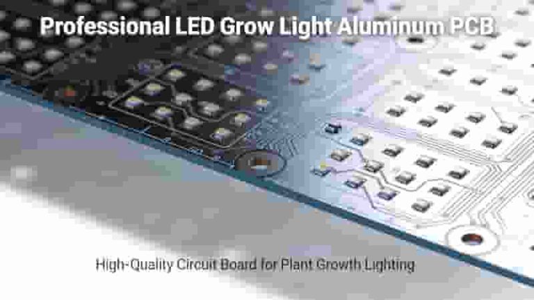
Rigid-Flex PCB manufacturing integrates flexible circuits and rigid boards to deliver compact, high-reliability interconnect solutions for medical, aerospace, automotive and industrial electronics. This professional guide covers full fabrication flow, material selection, DFM rules, quality control and industry best practices for global engineers and buyers.
What Are Rigid-Flex PCBs?
Rigid-flex PCBs are hybrid circuit boards that combine the flexibility of FPC with the structural stability of rigid PCBs. They eliminate bulky connectors, reduce assembly weight, and greatly improve reliability in dynamic or high-vibration environments.
Unlike standard rigid boards or standalone flexible circuits, rigid-flex PCB manufacturing produces a unified structure that supports 3D packaging and tight-space installations.
These boards are widely used in mission-critical applications where consistent performance and miniaturization are non-negotiable.
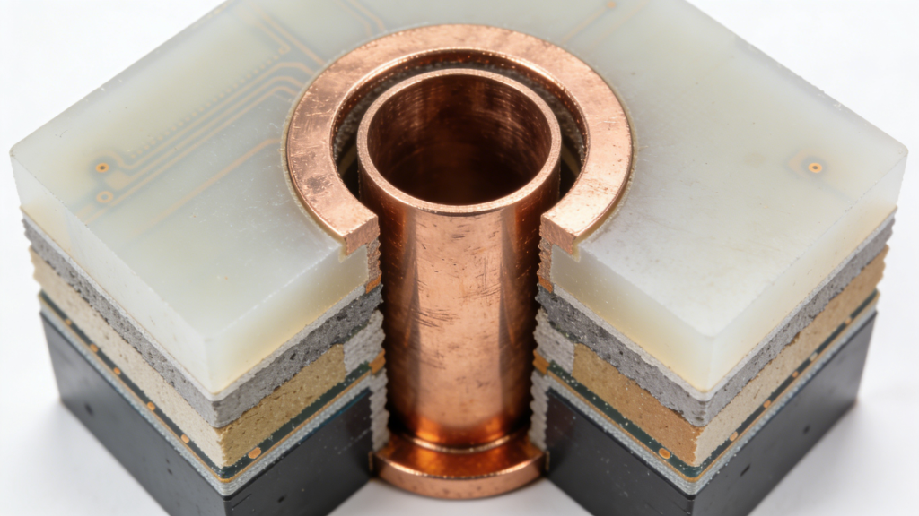
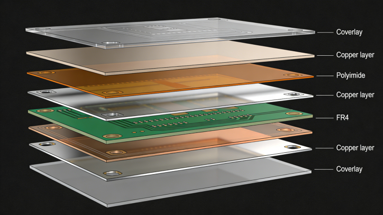
Structure & Core Materials
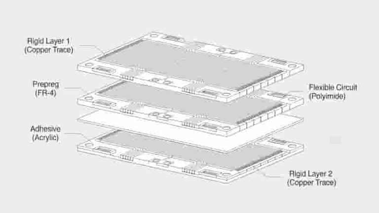
Typical Layer Structure
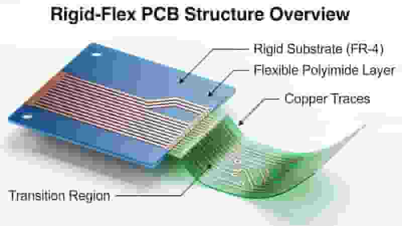
A standard rigid-flex board includes a flexible polyimide core, rigid FR4 sections, bonding prepreg, and protective coverlays. The flex area allows bending while rigid zones support SMD components.
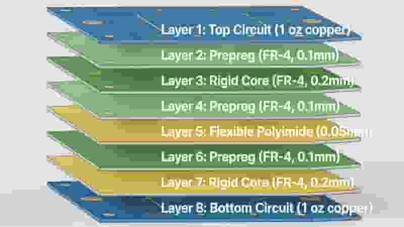
Key Materials in Rigid-Flex PCB Manufacturing
- Flex Core: High-temperature polyimide (DuPont Pyralux)
- Rigid Layers: FR4 standard or high-TG materials
- Prepreg: Bonding dielectric for layer lamination
- Coverlay: Protective film for flexible circuits
- Copper: Rolled annealed copper for flex zones
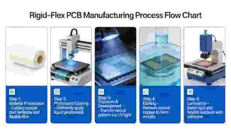
Full Rigid-Flex PCB Manufacturing Process
Rigid-flex PCB manufacturing is a precision multi-step process that requires tight control and advanced equipment.
1. Material Preparation
Cut FCCL, FR4, prepreg and coverlay to panel size. Selective copper removal ensures flex areas can bend safely.
2. Drilling
Mechanical drilling for through-holes and laser drilling for microvias down to 0.1 mm for HDI designs.
3. Circuit Generation
Photolithography and etching create precise circuits. LDI technology supports 30/30 µm trace width and spacing.
4. Coverlay Lamination
Protective coverlay is bonded to flex layers with controlled heat and pressure, then inspected by AOI.
5. Rigid Layer Lamination
Flex core and rigid FR4 layers are fused together under high-temperature pressing with accurate CCD alignment.
6. Black Hole & Plating
Conductive carbon layer applied to via walls, followed by copper plating to ensure stable interlayer connection.
7. Surface Finishing
Solder mask, silkscreen and surface finish (ENIG, HASL, etc.) protect circuits and improve solderability.
8. Opening Process
UV laser depth control exposes flex regions without damaging internal layers.
9. Testing & Quality Control
AOI, electrical testing, and four-terminal sensing ensure every board meets functional and reliability standards.
Rigid-Flex PCB Manufacturing Capabilities
| Parameter | Specification |
|---|---|
| Flex Layers | 1–6 layers |
| Total Rigid-Flex Layers | 2–32 layers |
| Min Trace / Space | 30 µm / 30 µm |
| Min Laser Via | 0.1 mm |
| Board Thickness | 0.5–6 mm |
Our rigid-flex PCB manufacturing supports HDI, high-frequency, and high-temperature applications with ISO-certified processes.
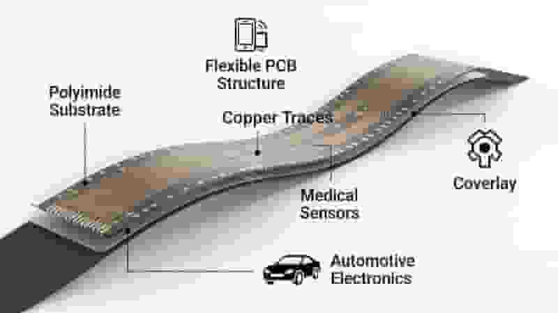
Key Industry Applications
Rigid-flex PCB manufacturing serves high-demand industries that require miniaturization and reliability:
- Medical: Pacemakers, hearing aids, wearable monitors
- Aerospace & Defense: Satellites, guidance systems, UAV components
- Automotive: EV battery management, ADAS sensors, infotainment
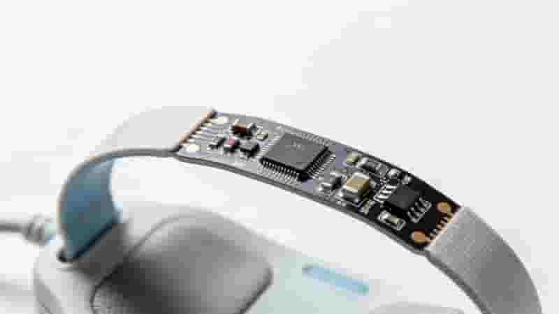
- Consumer Electronics: Smartwatches, AR/VR, wireless earbuds
- Industrial: Robotics, CNC equipment, control modules
Why Choose Us for Your Rigid-Flex PCB Projects
- Professional rigid-flex PCB manufacturing with mature process control
- LDI and UV laser systems for ultra-precision circuits
- Full DFM support to optimize your design for production
- ISO quality system and 100% electrical testing
- Quick-turn prototypes and mass production support
- One-stop service from design to assembly
Conclusion
Rigid-flex PCB manufacturing delivers the ideal balance of flexibility, stability and miniaturization for modern advanced electronics. With professional materials, precision equipment and strict quality control, we provide reliable solutions for global buyers in medical, automotive, aerospace and industrial fields.
Whether you need prototype development or mass production, we have the capabilities to support your project from design to delivery.
Start Your Rigid-Flex PCB Project Today
Request a free quote, DFM analysis or custom solution for your rigid-flex PCB manufacturing needs.
Get Free Quote
contact us for a free quote
Flexible PCB Manufacturing Process Steps: Complete Technical Guide
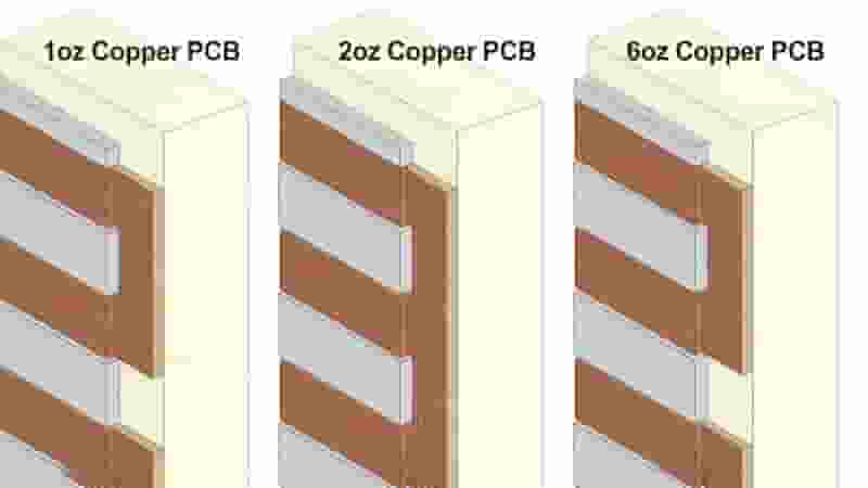
PCB Copper Thickness Capabilities | Standard & Heavy Copper (0.5oz to 15oz)
What is FR-4 Material in PCB Fabrication? The Complete Professional Guide
What is a Pad in PCB Design?
Flexible PCB Stiffeners: Materials, Benefits & Industrial Uses