This professional guide covers full flexible PCB manufacturing workflow, materials, key processes, quality control, and engineering best practices for global industrial buyers, engineers, and procurement teams.
What is Flexible PCB (FPC)
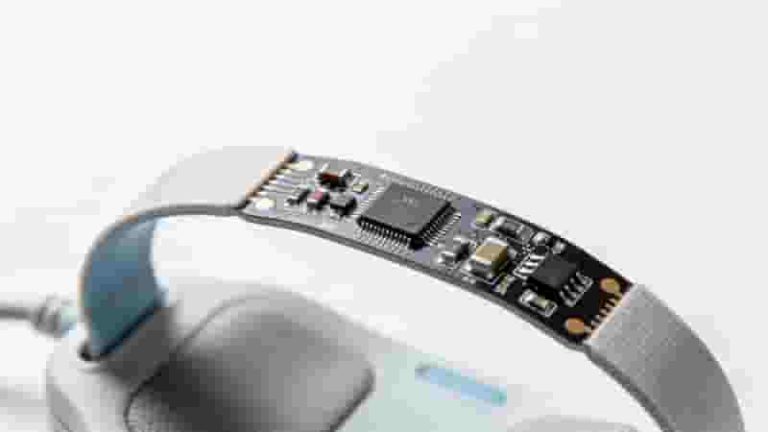
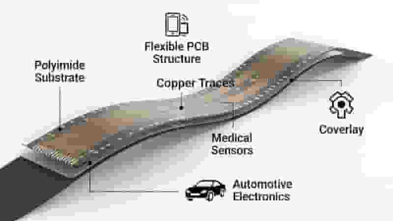
Flexible PCB (FPC) is a lightweight, bendable printed circuit board widely used in consumer electronics, automotive, medical devices, and industrial equipment. It supports component mounting and signal interconnection while adapting to dynamic bending and narrow installation spaces.
Unlike rigid PCBs, flexible PCB uses polymer films as substrates, offering excellent flexibility, thermal stability, and reliability. It is categorized by layer count: single-sided, double-sided, multilayer, rigid-flex, and specialized types.
Types & Stackup of Flexible PCB
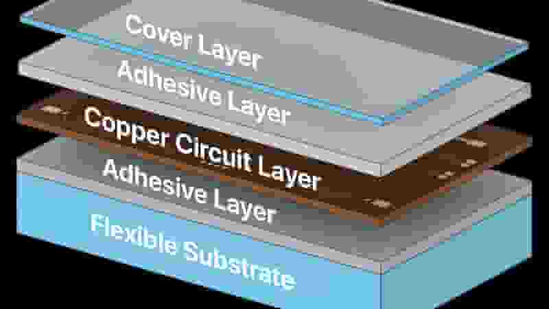
1. Single-Sided Flexible PCB
Low-cost structure with one conductive layer on flexible substrate. Ideal for simple circuits with low electrical performance requirements.
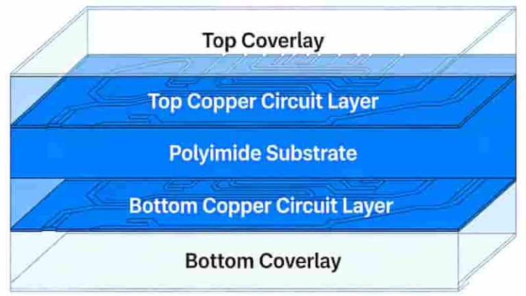
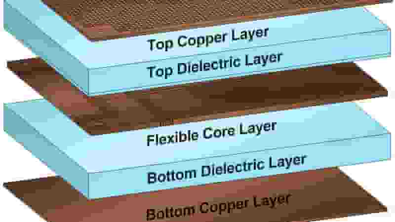
2. Double-Sided Flexible PCB
Conductive layers on both sides of the base film, connected by plated through holes (PTH). Suitable for moderate-complexity designs.
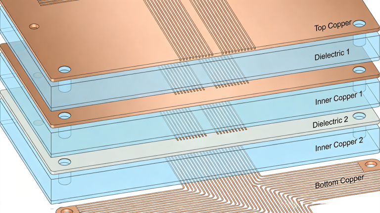
3. Multilayer Flexible PCB
3+ layers of single or double FPC bonded together with interlayer vias. Delivers high reliability, thermal performance, and routing density.
4. Rigid-Flex PCB
Combines rigid and flexible substrates for compact, high-strength assemblies used in aerospace, automotive, and medical devices.
5. Air Gap & Sculptured Flexible PCB
Specialized structures for high-density interconnection, LCD bonding, and floating contact applications.
Core Materials for Flexible PCB Manufacturing
The performance of flexible PCB manufacturing depends on high-quality raw materials:
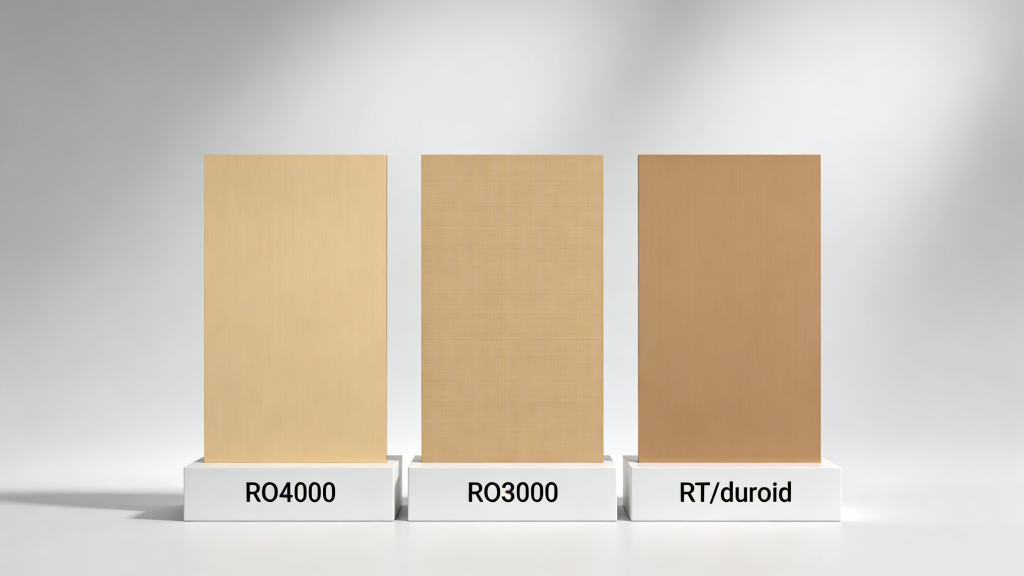
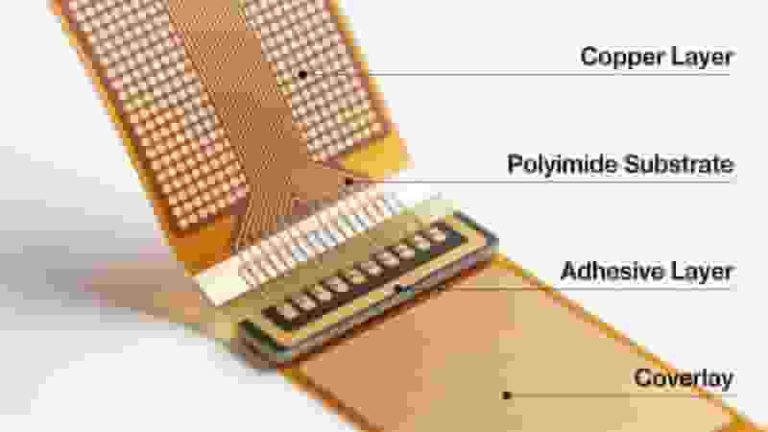
- Flexible Copper Clad Laminate (FCCL): PI/PET/PEN/LCP base films with electrolytic or rolled copper foil
- Coverlay (CVL): Protective insulating film for circuits
- Adhesive: Bonding material for multilayers and components
- Stiffeners: FR4, metal, or plastic for mechanical support
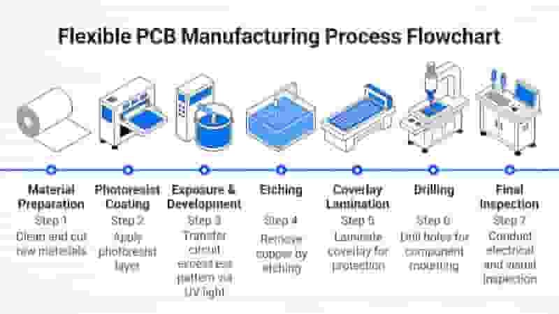
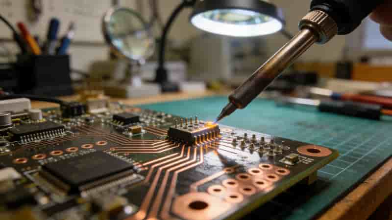
Complete Flexible PCB Manufacturing Process Steps
- Cutting: Cut FCCL to required panel size
- CNC Drilling: Drill vias and mounting holes
- Plasma Etchback: Clean hole walls and remove contaminants
- Black Hole / Shadow Process: Deposit conductive carbon layer
- Chemical Cleaning: Clean and roughen copper surface
- PTH (Plating Through Hole): Plate copper to connect layers
- Dry Film Lamination: Apply photosensitive resist
- Exposure & Development: Transfer circuit pattern
- Pattern Etching: Remove unwanted copper
- Dry Film Stripping: Remove resist to reveal circuits
- AOI Inspection: Check for open/short circuits
- Coverlay Lamination: Laminate protective film
- Hot Press Lamination: Bond layers under high temperature and pressure
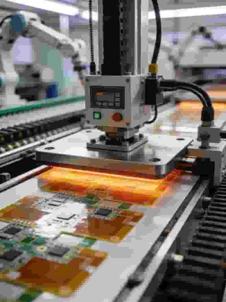
- Surface Finish: Immersion gold, tin, OSP, etc.
- Silkscreen: Print labels and symbols
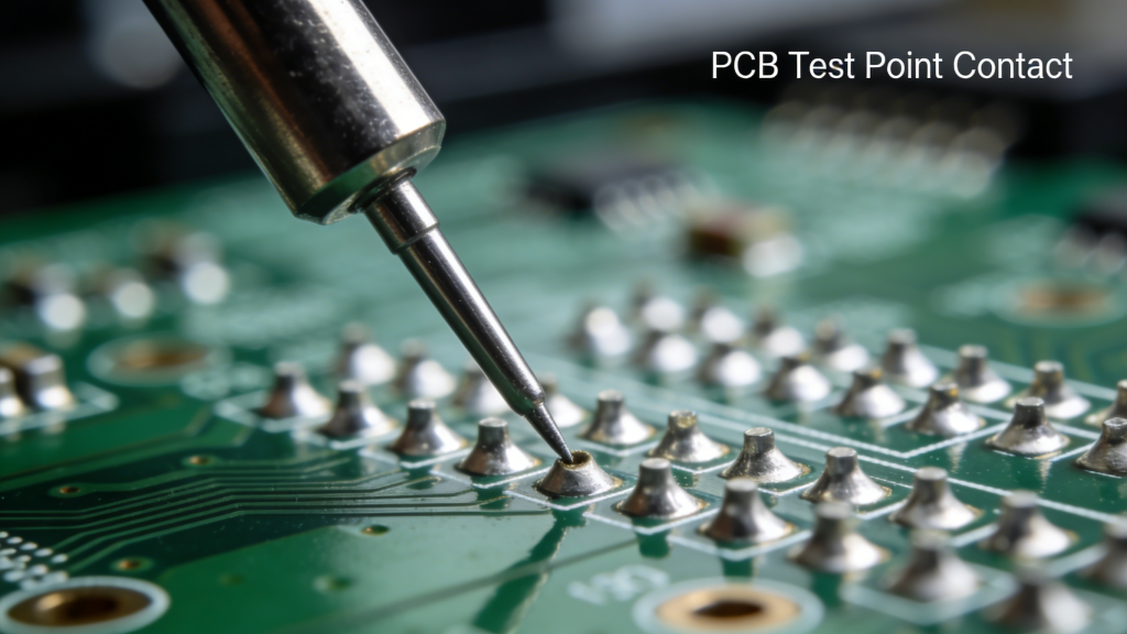
- Electrical Test: Verify open/short circuits
- Punching / Routing: Profile to final shape
- Final Inspection & Packaging: Visual, dimensional, and reliability check
Single-Sided vs Double-Sided FPC Process
| Process | Single-Sided FPC | Double-Sided FPC |
|---|---|---|
| Layer Structure | One conductive layer | Two conductive layers with PTH |
| PTH Process | Not required | Required |
| Complexity | Low | Medium |
| Cost | Lower | Moderate |
Quality Control & Testing in Flexible PCB Manufacturing
Professional flexible PCB manufacturing requires strict quality control:
- AOI automatic optical inspection
- Electrical open/short test
- Impedance test (for high-speed designs)
- Solderability and adhesion test
- Environmental reliability test (temperature cycling, humidity)
Summary
Understanding flexible PCB manufacturing process steps helps engineers and buyers evaluate suppliers, optimize design, and ensure product reliability. A complete, standardized process ensures stable performance, consistent quality, and cost efficiency for global industrial applications.
Need Custom Flexible PCB Solutions?
We provide professional flexible PCB manufacturing, prototyping, and assembly for global buyers. Request a free quote, drawing review, or technical consultation today.
Get Free Quote & Consultation
What Is the Difference Between PTH and Via in PCBs?
Flying Probe Testing for PCB: The Complete Professional Guide
High-Reliability PCBs For New Energy Applications
What is a Blank PCB? Buy Bare Circuit Boards | Layer PCB
High TG PCB Material: Thermal Stability, Key Benefits, Industrial Applications & Professional Fabrication Solutions