Bill of Materials (BOM) is the foundational document for PCB assembly and PCBA manufacturing. It lists all components, quantities, specifications, and reference details to ensure accurate sourcing, smooth production, and error-free assembly. This professional guide helps industrial buyers, engineers, and procurement teams create a complete, standardized PCB BOM for reliable prototyping and mass production.
What Is a PCB Bill of Materials (BOM)
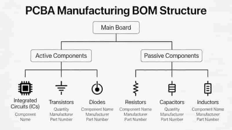
A PCB BOM is a structured, itemized list of every electronic component, hardware, and material required to build a printed circuit board assembly. It acts as the single source of truth for SMT assembly, through-hole assembly, and full PCBA manufacturing.
Unlike general BOMs, a PCB BOM includes manufacturer part numbers (MPN), reference designators, quantities, packaging, and component specifications to eliminate ambiguity in production.
Why BOM Is Critical for PCB Assembly
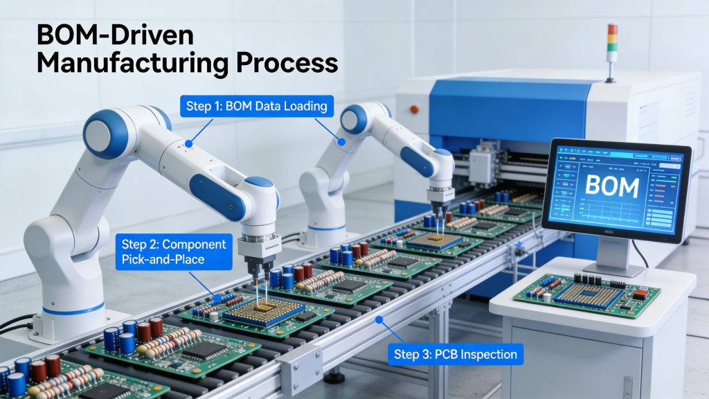
A correct PCB BOM directly improves efficiency, cost control, and quality in PCBA manufacturing:
- Standardizes component sourcing and reduces lead time
- Enables precise cost estimation and budgeting
- Minimizes assembly errors and rework in SMT assembly
- Supports inventory planning and supply chain stability
- Ensures compliance with IPC, RoHS, and quality standards
Essential Items in a PCB BOM
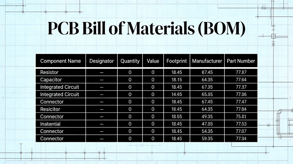
A professional PCB BOM must include these core fields for industrial PCB assembly:
- Item No.: Sequential identifier
- Manufacturer Part Number (MPN): Unique component ID
- Alternate MPN: Backup parts to avoid shortages
- Quantity: Required number per board
- Reference Designator: C1, R2, U3, etc.
- Component Description: Value, package, rating, type
- Manufacturer Name: Official brand
- Notes: Special requirements like RoHS or lead-free
PCB BOM Sample Table
| Item | MPN | Manufacturer | Qty | Designator | Description |
|---|---|---|---|---|---|
| 1 | GRM188R71H104KA93D | Murata | 5 | C1,C5,C7 | 0.1uF 50V 0603 |
| 2 | CRCW060310K0FKEA | Vishay | 2 | R1,R2 | 10kΩ 1% 0603 |
Step-by-Step to Create a PCB BOM
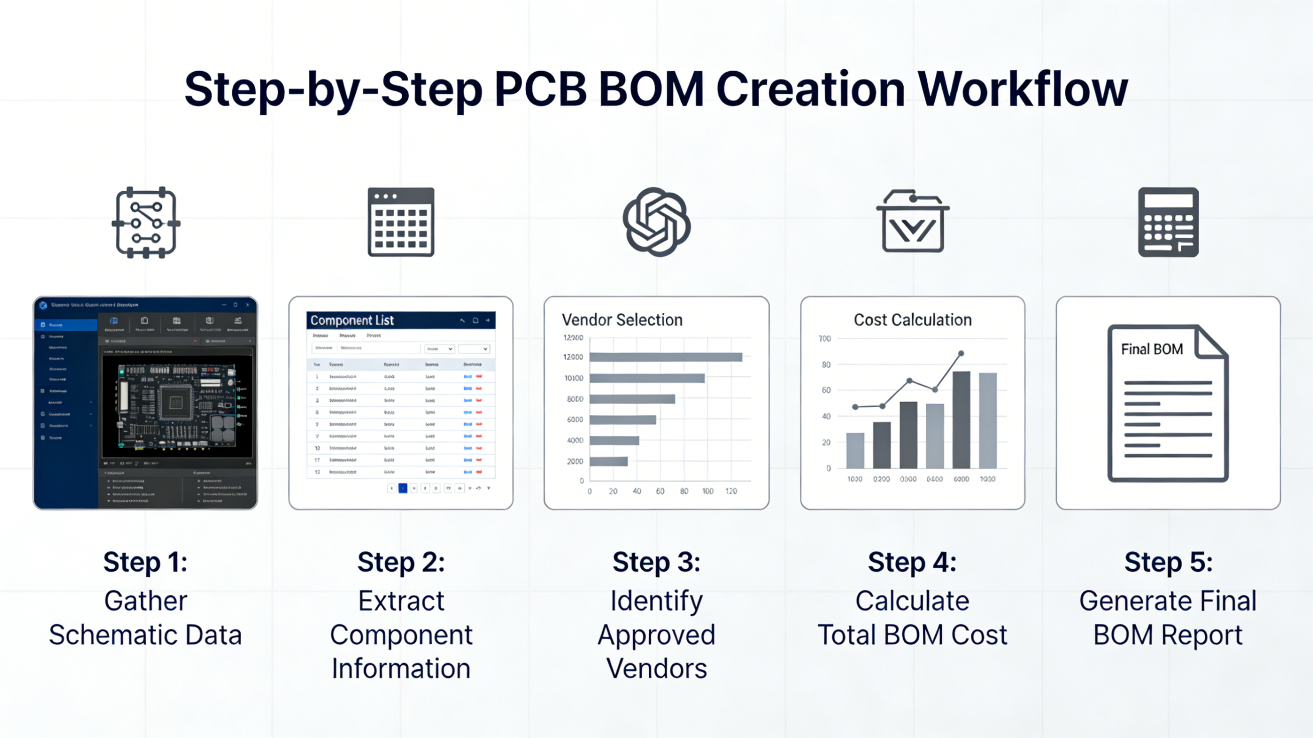
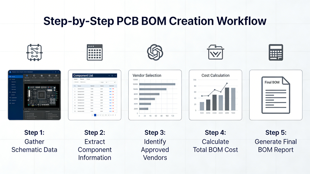
Follow this industry-standard workflow to build a reliable PCB BOM for PCB assembly:
- Export base data from PCB design software (Altium, KiCad, Eagle)
- Format into Excel or CSV with standard BOM columns
- Fill MPN, manufacturer, quantity, and reference designators
- Add component descriptions, package, and ratings
- Include alternate MPNs for high-risk components
- Validate parts availability on Digi-Key, Mouser, or LCSC
- Check for obsolete or end-of-life components
- Finalize and save as Excel/CSV for manufacturing
Common BOM Mistakes & Fixes
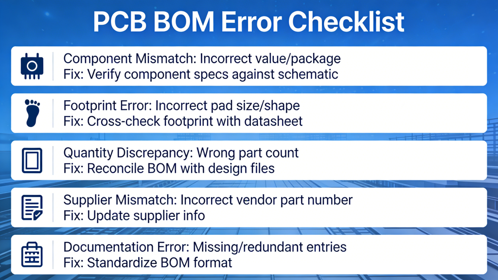
Avoid these errors that delay PCBA manufacturing and increase costs:
- Wrong MPN: Verify with datasheets; add alternates
- Missing reference designators: Match schematic and Gerber files
- Incorrect quantities: Recalculate and add 1–2% spares
- Obsolete components: Check Octopart or distributor sites
- Vague descriptions: Include value, package, voltage, tolerance
Tools for PCB BOM Creation
Use these professional tools to improve PCB BOM accuracy and efficiency:
- PCB Design: Altium Designer, KiCad, Eagle
- BOM Management: OpenBOM, Arena PLM, OrCAD
- Spreadsheet: Excel, Google Sheets (CSV/XLSX)
- Component Validation: Digi-Key, Mouser, Octopart
Conclusion & Next Steps
A well-built PCB BOM is the foundation of reliable, cost-effective PCB assembly and PCBA manufacturing. It reduces errors, speeds up production, and ensures consistent quality from prototyping to mass production.
By following industry standards and validating components carefully, you can avoid delays and control costs effectively.
Get Your Free BOM Review & PCB Assembly Quote
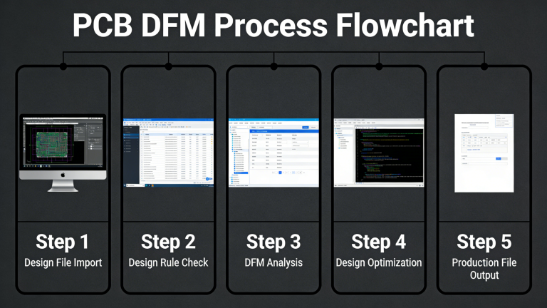
Send us your PCB BOM and Gerber files for a professional review, DFM analysis, and competitive quote for SMT assembly and full PCBA services.
Inquire Now · Custom PCB Assembly
What Are PCB Boards Made Of? Complete Materials Guide for Engineers & Buyers
Heat Resistant Circuit Boards: High-Temperature PCB Solutions for Industrial & Automotive Applications
High-Precision PCB & SMT Stencil Manufacturing
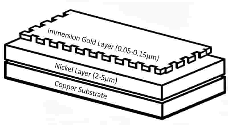
PCB Immersion Gold (ENIG) Surface Finish: Full Guide for Reliable Lead-Free PCBs
Single Layer PCB Manufacturing | Affordable Single Sided PCBs