Standard PCB thickness is typically 1.57 mm (0.062 inches), often rounded to 1.6 mm. This guide covers definitions, influencing factors, manufacturing constraints, non-standard design rules, and selection tips for industrial buyers and engineers.
Quick Overview: standard PCB thickness (1.6mm) is industry default; common alternatives include 0.78mm (0.031in) and 2.36mm (0.093in). Thickness impacts durability, weight, assembly, and reliability.
What Is Standard PCB Thickness?
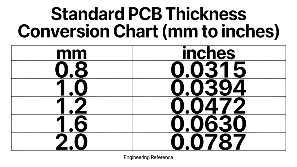
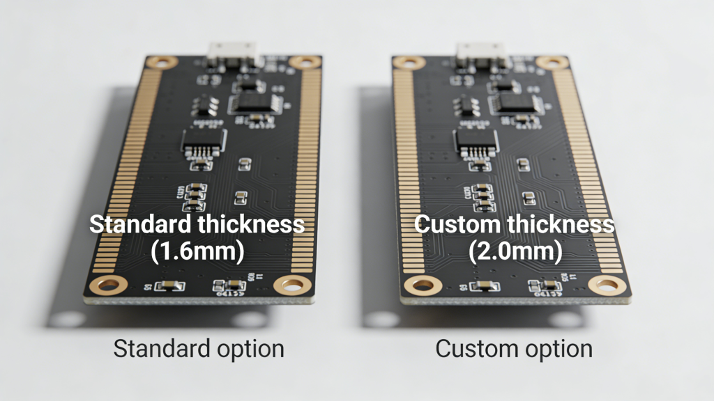
The industry standard PCB thickness is 1.57 mm (0.062 inches), universally referred to as 1.6 mm for simplicity. This dimension is compatible with most connectors, enclosures, and assembly processes.
Other widely used thicknesses:
- 0.78 mm (0.031 inches) – thin boards for compact devices
- 2.36 mm (0.093 inches) – thick boards for high-power or rugged use
The final thickness depends on assembly needs, layer count, and application environment.
Key Factors That Affect PCB Thickness
1. Copper Thickness
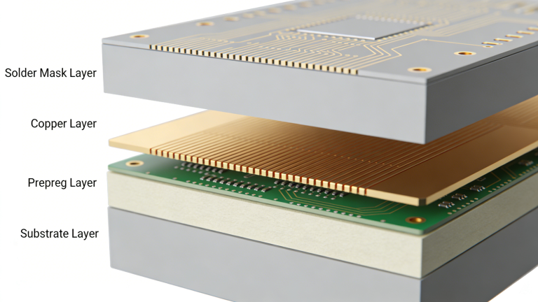
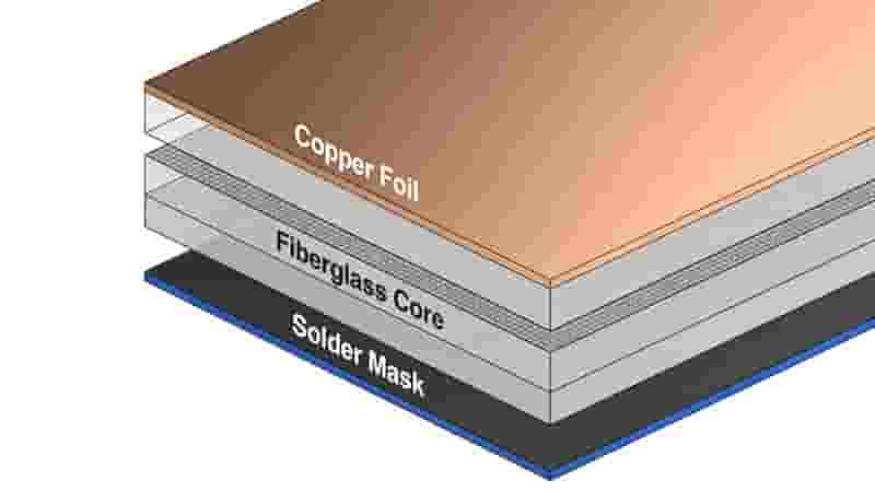
Standard copper weight is 1–2 oz (1.4–2.8 mils). Copper thickness directly affects current capacity and total board thickness. Thicker copper increases cost and final thickness.
2. Substrate Material
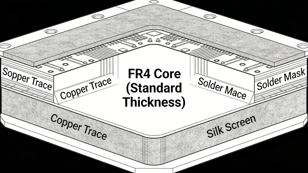
Dielectric materials like FR-4, G-10, and IMS form the core structure. Laminate thickness and Tg value determine the base thickness of the PCB.
3. Number of Layers
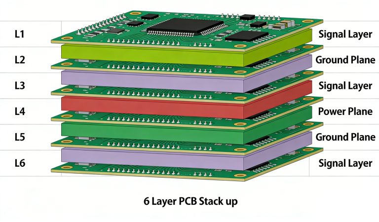
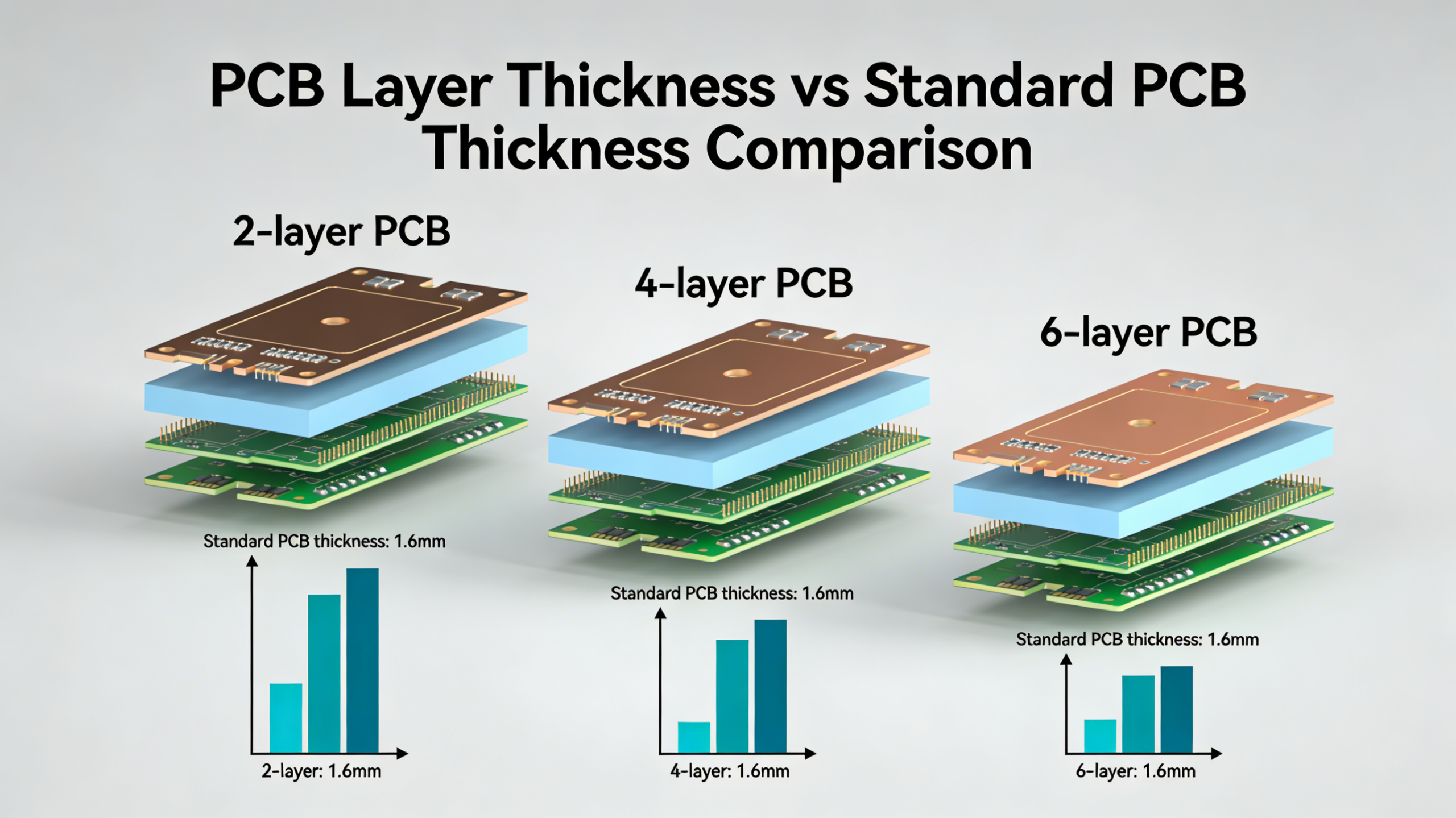
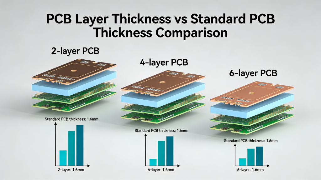
2–6 layer boards often use standard PCB thickness (1.6mm). Boards with 8+ layers require greater thickness to maintain reliability and manufacturability.
4. Signal & Power Requirements
High-power circuits need thicker copper and reinforced substrates, increasing overall thickness. High-frequency signals may require controlled dielectric thickness.
5. Via Type & Density
Through vias, microvias, blind vias, and buried vias affect minimum thickness and aspect ratio limits.
6. Operating Environment
Thicker boards perform better in high-vibration, high-temperature, or high-humidity environments. Thin PCBs suit lightweight, low-stress applications.
Manufacturing Factors That Affect PCB Thickness
1. Drilling Aspect Ratio
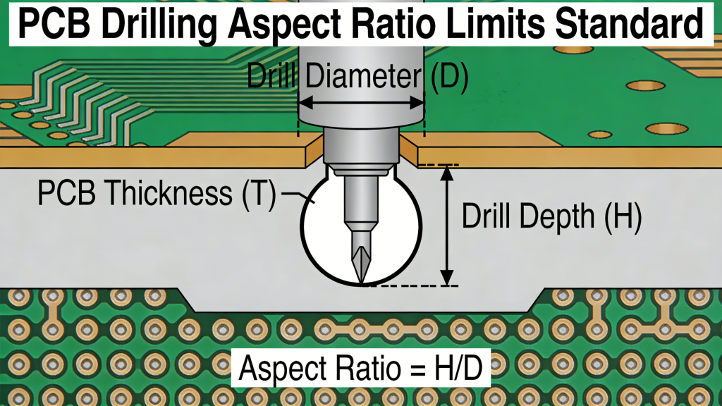
Standard drilling ratio is 7:1 (depth:diameter). Exceeding this requires special processes and raises costs. Thickness is limited by machine capability.
2. Copper Plating & Etching
Inner-layer copper thickness impacts lamination and final board dimension. Plating uniformity affects tolerance control.
3. Lamination Process
Multilayer lamination compresses materials slightly. High-layer-count boards cannot maintain standard PCB thickness without compromising quality.
Considerations for Non-Standard Thickness PCBs
When designing outside standard PCB thickness, verify these points:
- Factory capability: minimum 0.3mm, maximum 3.0mm thickness supported
- Additional cost for custom thickness and special processes
- Connector, component, and enclosure compatibility
- Mechanical strength and reliability testing
Standard PCB Thickness Comparison Table
| Thickness (mm) | Thickness (inch) | Typical Use | Layer Count |
|---|---|---|---|
| 0.78 | 0.031 | Compact consumer electronics | 1–2 layers |
| 1.6 (Standard) | 0.062 (Standard) | General industrial, commercial | 2–6 layers |
| 2.36 | 0.093 | High-power, rugged devices | 4–8+ layers |
Summary
Standard PCB thickness (1.6mm / 0.062in) is the most cost-effective and widely compatible choice for most applications. Thickness is determined by copper weight, substrate, layer count, vias, signal needs, and manufacturing limits.
Non-standard thicknesses are available for specialized use but require factory confirmation and may add cost. Always match thickness to assembly, environment, and performance requirements.
Request a Custom PCB Quote
We provide standard and custom thickness PCBs from 0.3mm to 3.0mm, supporting prototyping and mass production. Our ISO, UL, and RoHS certified facilities ensure stable quality and fast delivery.
Tell us your layer count, copper weight, substrate, target thickness, and quantity. We will send a free DFM check and detailed quote within 24 hours.
Get Free Quote Now
Flexible PCB: Full Guide to Materials, Design & Applications
High Volume PCB Assembly Services
Double Sided PCB Manufacturing: Process, Specifications & Custom Solutions
Understanding Plated Half-Holes (Castellated Holes) in PCB Design
Aluminum PCB vs FR4 PCB: Full Technical Comparison for Industrial & Export Buyers