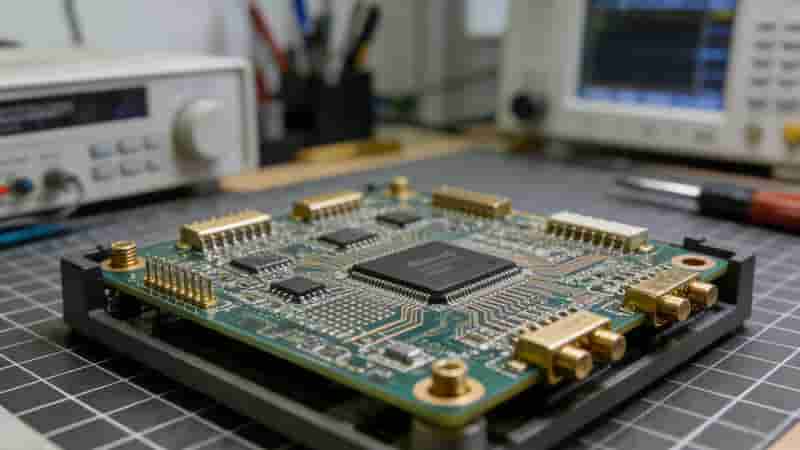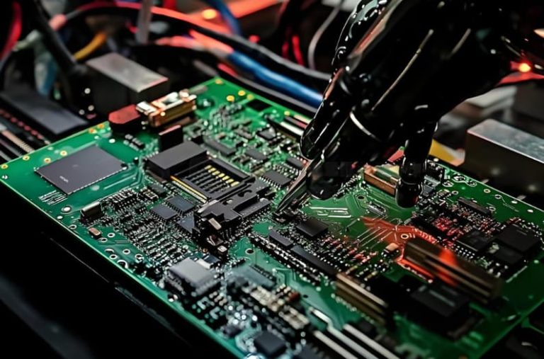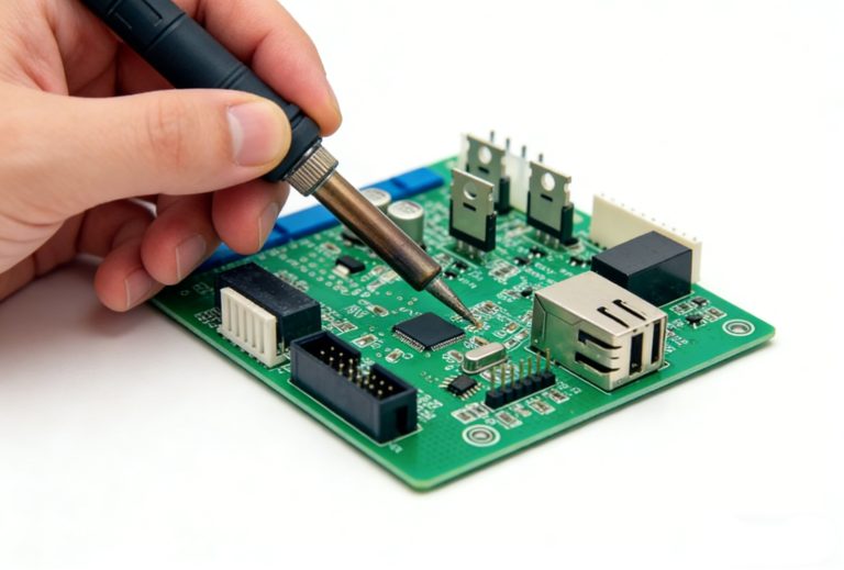
A Surface Mount Device (SMD) component package is a standardized enclosure designed for direct soldering onto PCB surfaces, enabling high-density assembly, miniaturization, and automated manufacturing in modern electronics.
What Is an SMD Component Package?
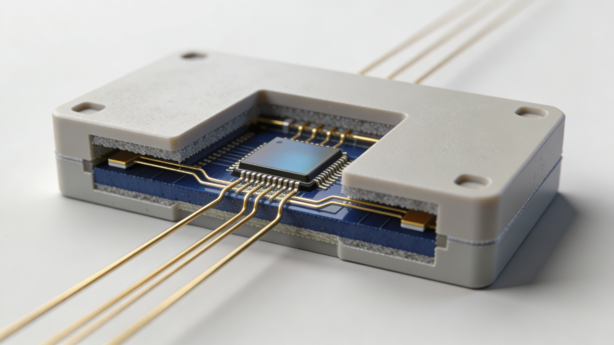
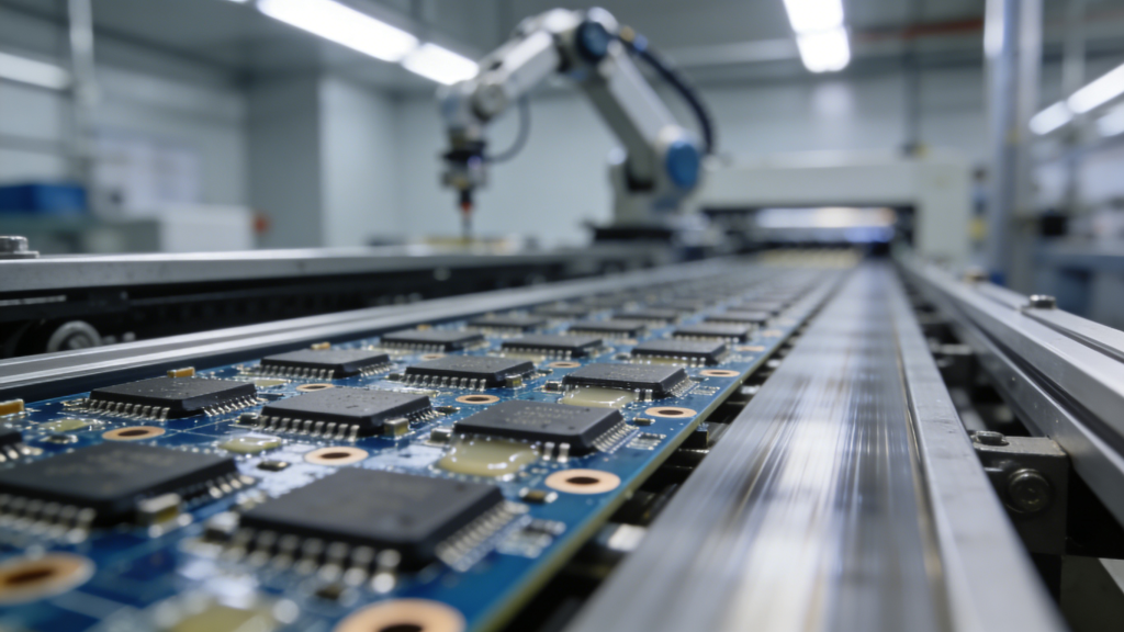
SMD stands for Surface Mount Device, referring to electronic components designed exclusively for Surface Mount Technology (SMT) assembly. An SMD component package is the physical housing that protects internal chips, provides electrical connections, supports heat dissipation, and enables automated placement onto printed circuit boards.
Unlike through-hole components, SMD packages require no drilled holes. They are soldered directly to copper pads on PCB surfaces, making them the foundation of compact, high-performance electronic devices.
Key Differences: SMD vs SMT
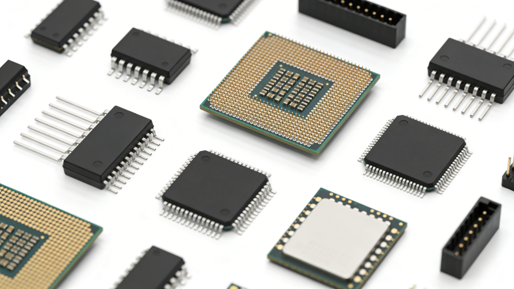
Many people confuse SMD and SMT. Here is a clear distinction:
- SMD: Surface Mount Device – the actual electronic component used in assembly
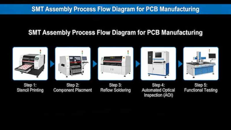
- SMT: Surface Mount Technology – the automated process of mounting SMD components onto PCB
| Term | Full Name | Category |
|---|---|---|
| SMD | Surface Mount Device | Component |
| SMT | Surface Mount Technology | Assembly Process |
| SMC | Surface Mount Component | Component |
| SMP | Surface Mount Package | Component Housing |
Advantages of SMD Components & SMT
SMD components and SMT assembly dominate modern electronics manufacturing due to these benefits:
- Up to 60-80% smaller size and lighter weight than through-hole parts
- Higher PCB assembly density for compact device design
- Better high-frequency performance and lower electromagnetic interference
- Stronger anti-vibration and higher reliability with low solder defect rates
- Fully automated production supporting mass manufacturing
- Cost reduction of 30-50% through material and labor savings
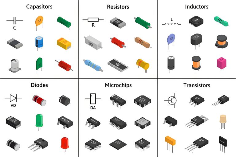
Common Types of SMD Components
Passive Components
- Chip Resistor (R): Standard surface mount resistors with compact SMD packages
- MLCC Capacitor (C): Multi-layer ceramic capacitors, the most widely used SMD component
- Inductor (L): Compact coil components for filtering and energy storage
- Crystal Oscillator (X): Provides stable clock signals for circuits
Active Components
- Diode / LED (D): Rectification and lighting functions in small SMD packages
- Transistor (Q): SOT-23, SOT-223 packages for switching and amplification
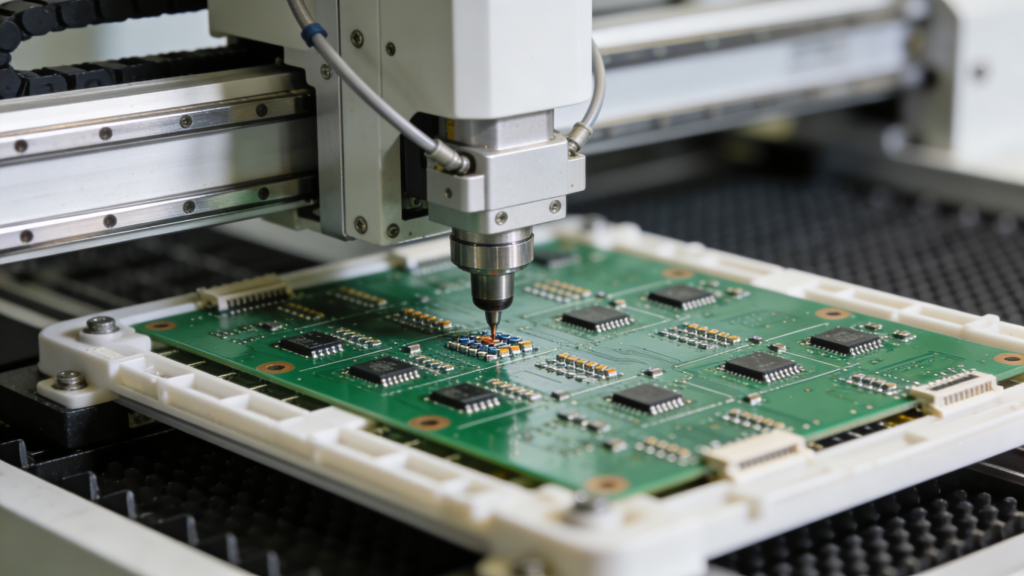
- Integrated Circuit (IC): Complex functions in QFP, BGA, CSP SMD packages
Main SMD Component Package Types
- SOP / SOIC: Small Outline Package – standard low-pin ICs
- QFP: Quad Flat Package – high-pin-count logic ICs
- BGA: Ball Grid Array – high-performance processors with bottom solder balls
- CSP: Chip Scale Package – near-chip-size SMD packaging
- LCCC / CLCC: Leadless ceramic chip carriers for high-reliability use
- QFN: Quad Flat No-leads – compact, thermally efficient SMD package
Standard SMD Component Sizes (Imperial & Metric)
| SMD Size | Metric (mm) | Inch |
|---|---|---|
| 1206 | 3.2 × 1.6 | 0.12 × 0.06 |
| 0805 | 2.0 × 1.25 | 0.08 × 0.05 |
| 0603 | 1.6 × 0.8 | 0.06 × 0.03 |
| 0402 | 1.0 × 0.5 | 0.04 × 0.02 |
| 0201 | 0.6 × 0.3 | 0.02 × 0.01 |
SMD Storage, Handling & Inspection
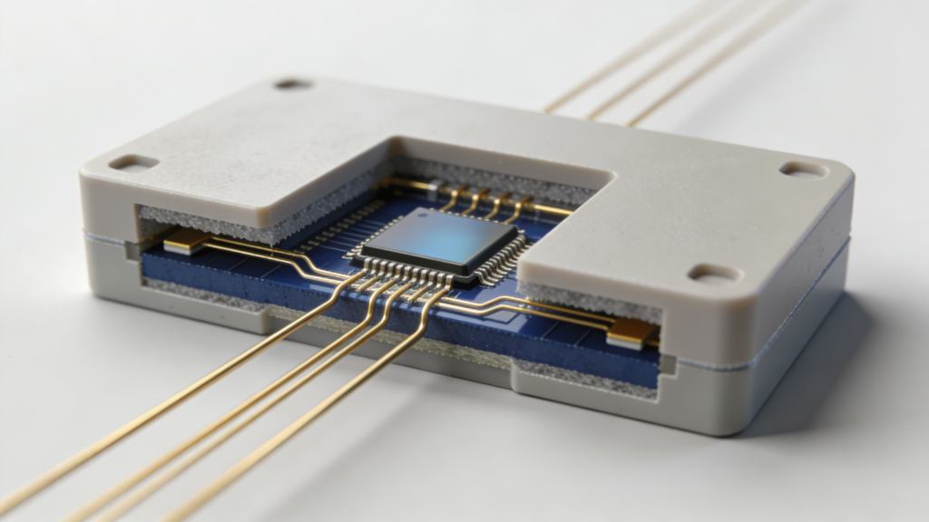
Proper management of SMD components ensures reliable PCB assembly:
- Store in ≤30°C, ≤75% RH environment to prevent moisture damage
- Use opened moisture-sensitive devices within 12-48 hours
- Bake components at 125°C ±5°C if humidity indicator exceeds 30%
- Inspect solderability, pin coplanarity, and absence of oxidation
Conclusion
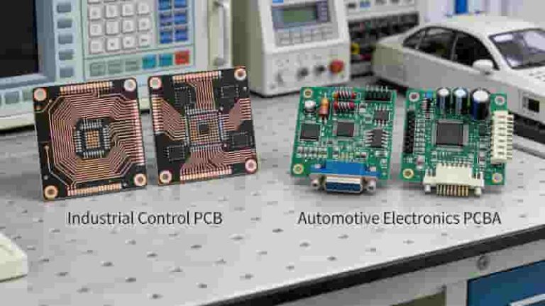
A Surface Mount Device (SMD) component package is essential to modern PCB design and manufacturing. It enables miniaturization, high performance, and mass production for consumer, industrial, and automotive electronics.
Understanding SMD packages, sizes, and assembly requirements helps engineers and purchasers select optimal components for reliable, cost-effective PCB projects.
Need Professional SMD PCB Assembly?
We provide full SMT assembly, SMD component procurement, and turnkey PCB solutions for global buyers. Get fast quotes, reliable quality, and on-time delivery.
Request a Quote Now
Multilayer PCB Manufacturing Services in China | High-Reliability PCB Solutions
Rapid PCB Prototyping and Production: Accelerate Your Product Launch
30 Common SMT PCB Assembly Defects: Causes, Impacts & IPC-Compliant Prevention
PCB Vias Explained: Through, Blind, and Buried Holes
Fast Turnaround PCB Prototype Services from Certified Manufacturer