Selective wave soldering is a precision soldering method designed for mixed-technology PCBs, protecting heat-sensitive components while delivering reliable through-hole solder joints. This professional guide covers core principles, process flow, critical parameters, DFM rules, defect resolution, and quality control for industrial PCB manufacturing.
1. Overview of Selective Wave Soldering
The two primary process technologies in PCB assembly are Surface Mount Technology (SMT) and Through-Hole Technology (THT), using reflow soldering and wave soldering respectively. As assembly technology advances, selective wave soldering has become a preferred solution for modern PCB manufacturing.
Selective wave soldering targets specific THT components without exposing the entire PCB to molten solder. It solves the limitations of reflow soldering for temperature-sensitive devices and supports lead-free processes, making it widely used in automotive, industrial, aerospace, and high-reliability electronics.
Unlike conventional wave soldering, which immerses the full board, selective soldering applies solder only to designated pads and pins. This precision protects nearby components and reduces material waste while improving joint quality.
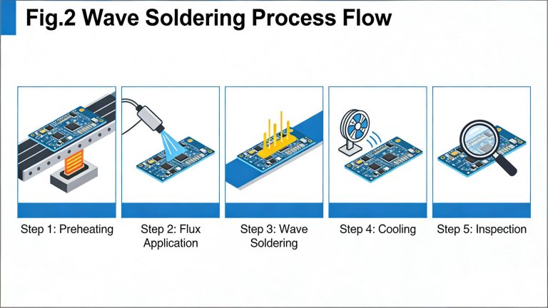
2. Core Process Flow
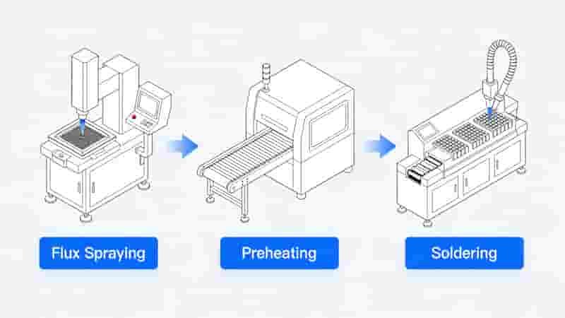
A complete selective wave soldering line includes three key stages:
2.1 Flux Coating
Precise flux application activates solder pads and prevents oxidation. Micro-droplet spray ensures no contamination on non-soldering areas. Typical deposition accuracy is 0.5 mm.
2.2 Preheating
Preheating evaporates flux solvents and reduces thermal shock. Temperature settings depend on PCB thickness, layer count, and component package type.
2.3 Soldering
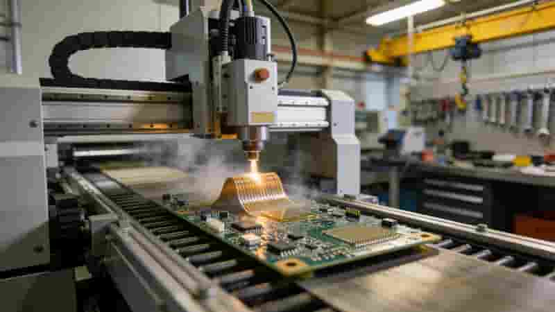
The PCB contacts a miniature solder wave under programmable control. Inert nitrogen gas is often used to minimize oxidation and improve wetting.
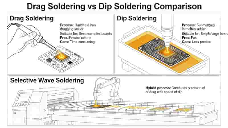
3. Process Types: Drag vs. Dip Soldering
3.1 Drag Soldering Process
Uses a single small-diameter solder nozzle (typically below 6 mm). The PCB moves across the solder wave at a controlled angle (0 to 12 degrees; recommended 10 degrees for most components). Ideal for dense boards and individual pins.
- Solder temperature: 275 to 300 degrees C
- Travel speed: 10 to 25 mm/s
- High precision and flexibility
- Better heat transfer than dip soldering
3.2 Dip Soldering Process
Uses multiple custom nozzles aligned with PCB solder points. All joints are soldered simultaneously, delivering throughput similar to traditional wave soldering. Best for high-volume runs with consistent layouts.
- Supports 0.7 to 10 mm solder joints
- Minimal bridging risk
- Lower equipment cost than robotic systems
- Requires custom nozzles per board design
4. Process Comparison Table
| Item | Selective Wave Soldering | Traditional Wave Soldering | Manual Soldering |
|---|---|---|---|
| Thermal Stress | Low, localized only | High, full board exposure | Variable, operator-dependent |
| Solder Usage | Minimized, efficient | High, large solder pot | Inconsistent |
| Component Protection | Excellent for heat-sensitive parts | Limited | Poor |
| Consistency | High, programmable | Good | Low |
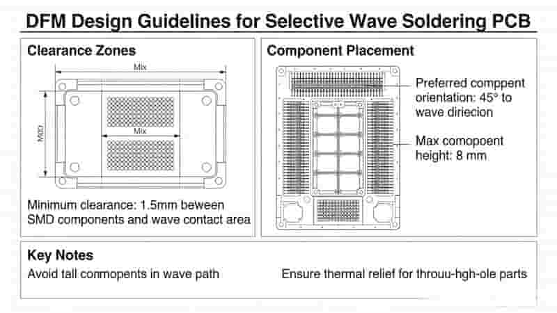
5. DFM & Design Guidelines
Follow these rules to optimize selective wave soldering performance:
- Maintain 5 mm or more clearance between solder joints and adjacent components
- Keep THT pin pitch consistent to simplify nozzle design
- Avoid tall components near soldering areas to prevent shadowing
- Use solder mask defined pads for better wetting control
- Design fixtures with 1.27 mm or more edge thickness to prevent solder leakage
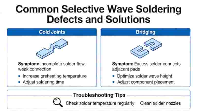
6. Defect Troubleshooting
Common issues in selective wave soldering and solutions:
- Cold joints / insufficient wetting: Increase solder temperature or extend contact time
- Bridging: Optimize nozzle speed, reduce flux volume, add nitrogen
- Poor through-hole filling: Check preheat profile and verify flux activation
- Pad lifting: Reduce thermal stress and lower peak temperature
7. Advantages & Limitations
Key Advantages
- Protects heat-sensitive SMT and THT components
- Lower energy and solder consumption
- High solder joint reliability and consistency
- Compatible with lead-free processes
- Minimal PCB warpage due to localized heating
Limitations
- Requires dedicated equipment and programming
- Lower throughput for high-pin-count boards
- Needs clear keep-out zones around THT pins
8. Summary
Selective wave soldering is an essential process for high-mix, high-reliability PCB assembly. It balances precision, efficiency, and component protection better than traditional wave or manual soldering. By following proper process parameters and DFM rules, manufacturers can achieve consistent, high-quality THT connections for industrial, automotive, and aerospace applications.
Need Professional PCB Assembly Support?
We provide expert selective wave soldering and full PCB assembly services for industrial and high-reliability projects. Contact us for a free quote or technical consultation.