Explore multilayer PCBs: their structure, benefits, and applications. We deliver fast, high-quality multilayer PCB manufacturing and prototyping services for global industrial buyers and engineers.
What is a Multilayer PCB?
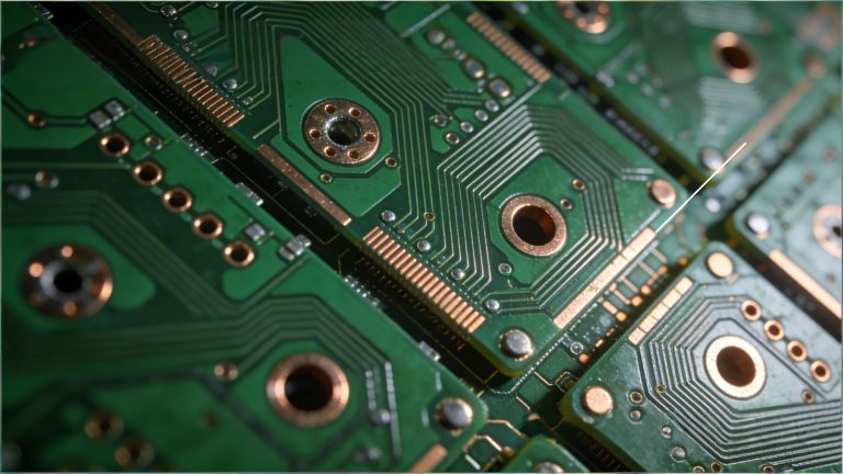
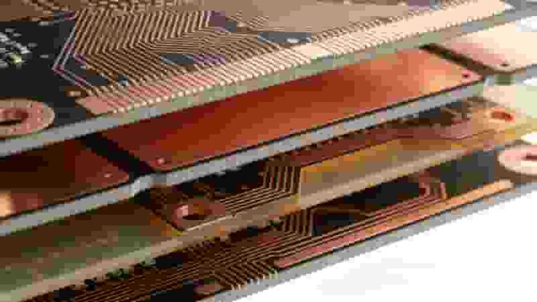
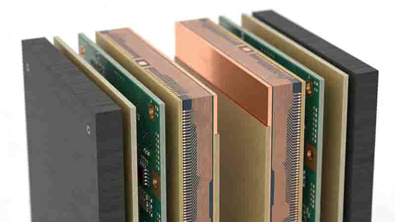
A multilayer PCB features three or more copper layers, unlike single-layer PCBs with just one. Components are placed on the outer surface layers, while inner layers manage wiring and connections, enabling compact and efficient circuit designs.
Benefits of Multilayer PCBs
Multilayer PCBs offer key advantages for modern electronics:
- Compact Size: Minimize space with a reduced form factor, ideal for small devices.
- Lightweight Design: Lighter boards simplify integration into portable products.
- Enhanced Durability: Multiple layers ensure long-term reliability under stress.
- Greater Flexibility: Adaptable for complex circuit layouts and applications.
- Improved EMI Shielding: Reduce interference for better signal integrity.
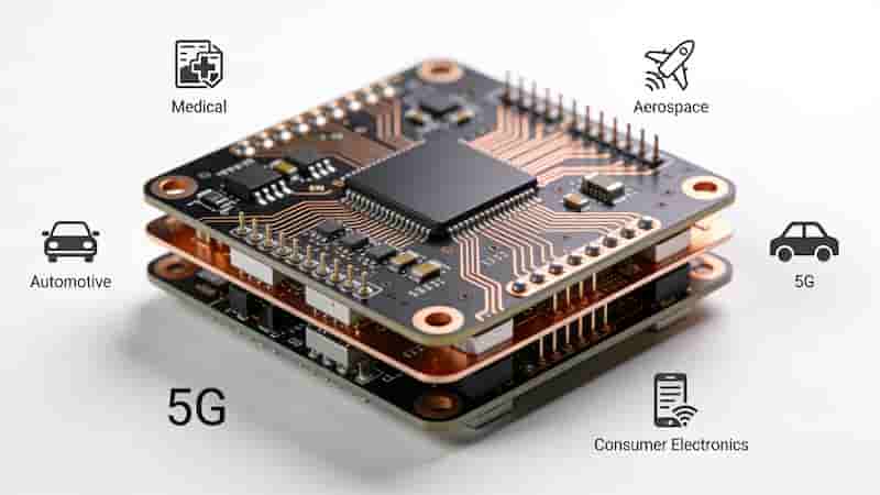
Multilayer PCB Applications
Multilayer PCBs power advanced technology across industries:
- Computers: Enable high-speed processing in compact motherboards.
- Medical Equipment: Support precision in diagnostic devices like MRI machines.
- Satellite & Aerospace: Ensure reliable communication and performance in extreme environments.
- Wearable Devices: Fit complex circuits into small, flexible designs.
- Defense: Provide durability for rugged military electronics.
- Telecommunication: Boost signal integrity in 5G infrastructure.
How Many Layers in a Multilayer PCB?
Multilayer PCBs range from 4 to over 100 layers, depending on complexity:
- 4–6 Layers: Ideal for consumer electronics like smartphones.
- 8–12 Layers: Used in advanced devices like medical equipment.
- Up to 100 Layers: Support high-density applications like aerospace systems.
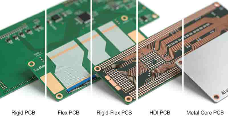
Types of Multilayer PCBs
- Multilayer Rigid PCB: Solid FR4 structure for stable, high-performance circuits.
- Flexible Multilayer PCB: Polyimide-based bendable boards for space-saving designs.
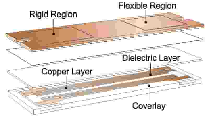
- Rigid-Flex Multilayer PCB: Combines rigid and flexible layers for hybrid designs.
- HDI Multilayer PCB: High-Density Interconnect for advanced miniaturization.
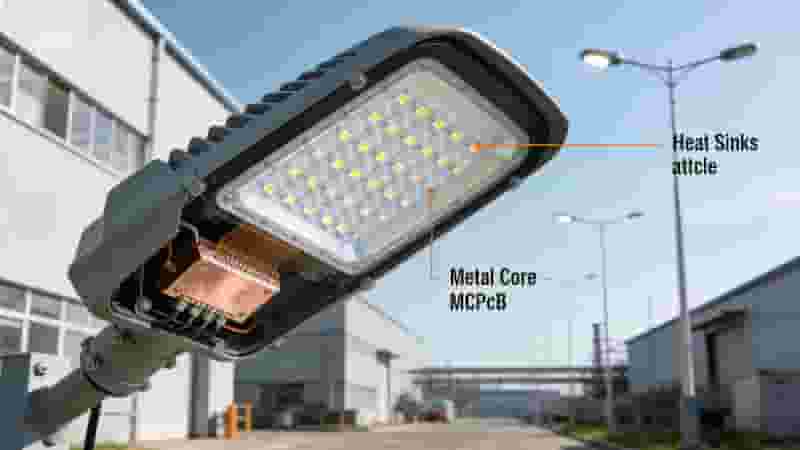
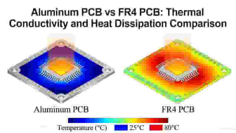
- Metal Core Multilayer PCB: Enhanced thermal management for high-power devices.
Single-layer vs Multilayer PCB Comparison
| Aspect | Single/Double-Layer PCB | Multilayer PCB |
|---|---|---|
| Space Efficiency | Bulky, limited for complex designs | Compact, high-density friendly |
| Connectivity | Requires jumpers | Streamlined via inner layers |
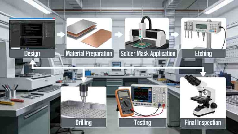
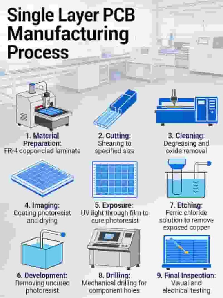
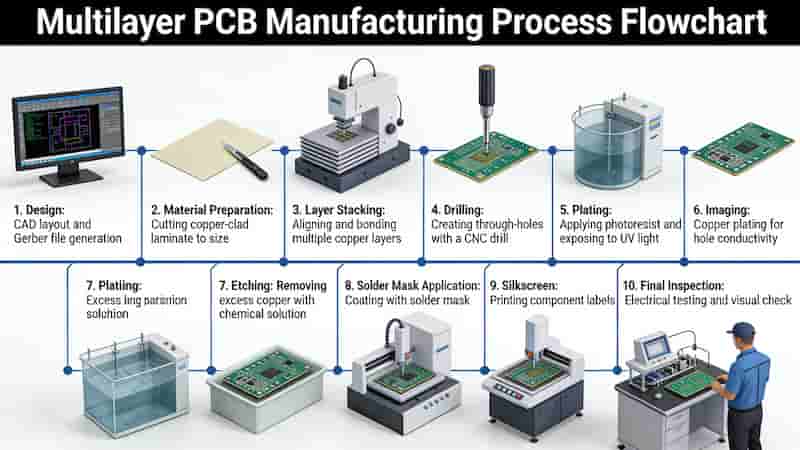
Multilayer PCB Manufacturing Process
Our multilayer PCB manufacturing follows strict IPC standards for precision and reliability:
- Design & Layout (CAD)
- Material Selection
- Inner Layer Imaging & Etching
- Lamination
- Drilling & Plating
- Outer Layer Processing
- Solder Mask & Silkscreen
- Surface Finish
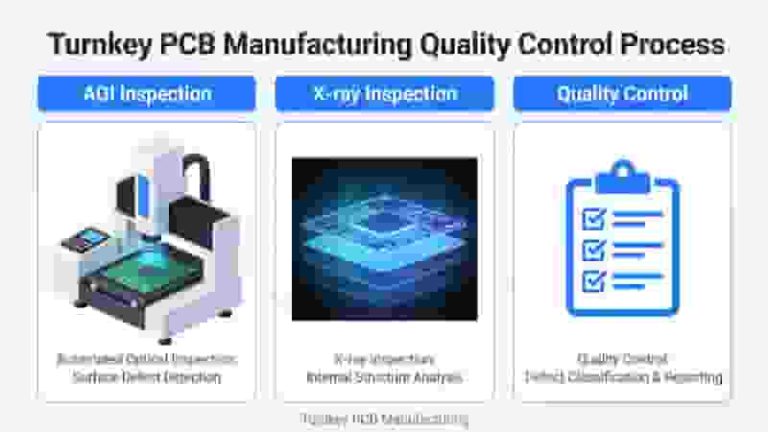
- Electrical Test & Quality Inspection
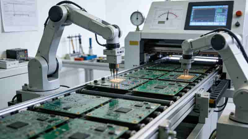
Our Multilayer PCB Manufacturing Capabilities
| Feature | Specifications |
|---|---|
| Layer Capacity | Rigid: up to 30 layers; Flex: up to 10 layers; Rigid-Flex: up to 8 layers |
| Materials | FR4, High Tg, High-frequency, Polyimide |
| Board Thickness | 0.1–6.0 mm |
| Surface Finish | Lead-free HASL, ENIG, Immersion Silver/Tin, Hard Gold |
| Testing | Impedance Control, AOI, Flying Probe, Thermal Shock |
Why Choose Our Multilayer PCB Services?
- Proven expertise in multilayer PCB prototyping and mass production
- Free DFM checks to optimize your design and reduce costs
- Advanced equipment ensuring consistent quality
- Fast lead times: prototypes as fast as 24–48 hours
- Worldwide shipping for global buyers and importers
Summary
Multilayer PCB technology is essential for modern compact, high-performance electronics. We provide full-cycle multilayer PCB prototyping & manufacturing services with strict quality control, fast lead times, and professional support for global industrial clients.
Request a Free Multilayer PCB Quote Today
Get a fast, customized quote for your multilayer PCB project. We support prototyping and mass production with global delivery.
Get Free Quote
PCB Terminology Glossary – Over 150 Essential PCB Terms for Engineers & Global Buyers
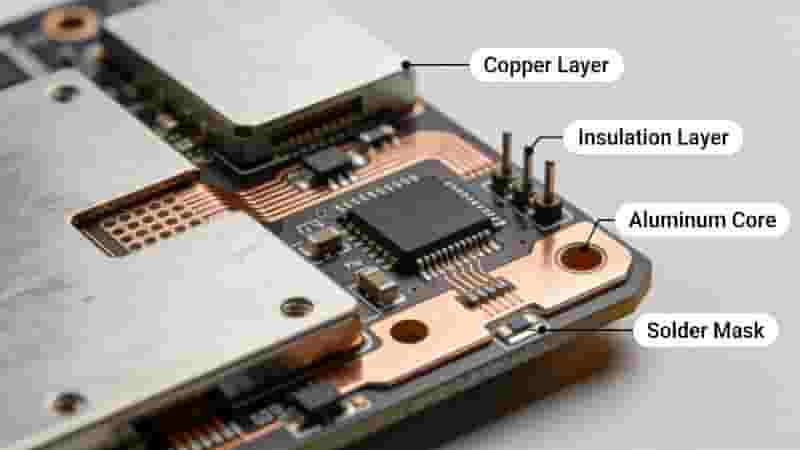
Copper Core PCB vs. Metal Core PCB: Key Differences & Advantages
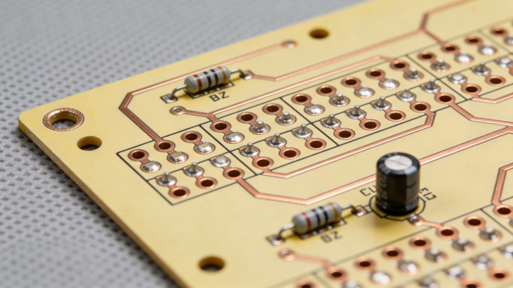
Single Layer PCB Manufacturing | Affordable Single Sided PCBs
Metal Core PCB (MCPCB) Manufacturing Service in China
Aluminum PCB vs FR4 PCB: Full Technical Comparison for Industrial & High-Power Applications