Multilayer PCB stackup and thickness directly determine signal integrity, EMC performance, mechanical stability and manufacturability. This professional guide covers core principles, key parameters, standard stackups from 4‑layer to 14‑layer, thickness selection and engineering best practices for industrial electronics, high‑speed designs and critical applications.
Why Multilayer PCB Stackup And Thickness Matter
Modern electronics demand smaller size, higher integration, faster signals and longer reliability. Multilayer PCB stackup defines the arrangement of copper signal layers, ground planes, power planes and dielectric materials. Thickness impacts mechanical strength, connector compatibility, thermal performance and assembly yield.
A well‑designed stackup improves EMI/EMC, signal integrity and power integrity, controls impedance and reduces crosstalk. Poor stackup leads to radiation, signal reflection, ringing and early failure even with correct schematics and layout.
This guide provides industry‑standard stackup examples, thickness ranges and selection rules to help engineers and buyers choose optimal configurations for high‑reliability production.
PCB Stackup Basics: Core, Prepreg & Copper Layers
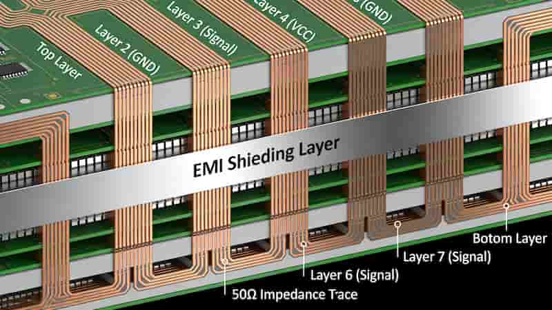
Multilayer PCB stackup is a structured combination of copper foils, core laminates and prepreg materials. Symmetrical design minimizes warpage and stress, critical for high‑layer and large‑format boards.
- Core: Rigid FR‑4 laminate with copper on both sides, providing mechanical stability and fixed dielectric thickness.
- Prepreg: Resin‑impregnated fiberglass used to bond layers and adjust dielectric thickness for impedance control.
- Copper Foils: 1 oz, 2 oz or heavier for signal routing, power distribution and thermal conduction.
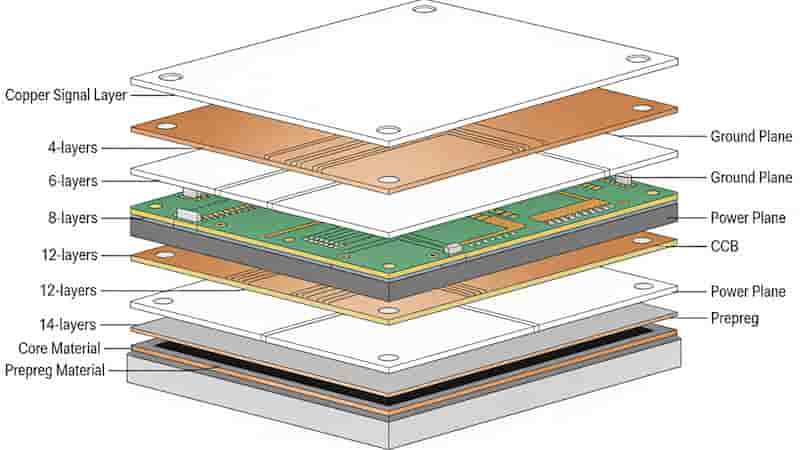
Balanced stackups mirror layers around the center, improving impedance consistency and reducing manufacturing defects.
Key Factors That Affect Multilayer PCB Thickness
Final board thickness results from electrical, mechanical and manufacturing constraints:
- Layer Count & Arrangement: More layers increase thickness; plane layers require minimum dielectric spacing.
- Core & Prepreg Thickness: Primary contributor to total thickness; selected for impedance and rigidity.
- Copper Weight: Heavier copper adds thickness and affects dielectric requirements.
- Impedance Control: High‑speed designs need precise dielectric thickness for 50Ω / 100Ω targets.
- Mechanical Constraints: Fits enclosure, connectors and rigidity needs.
- Thermal & Reliability: Thicker boards improve heat dissipation; material Tg and thickness prevent delamination.
- Manufacturing Standard: Standard thicknesses offer lower cost, faster lead time and higher yield.
Standard Thickness Options: 4‑Layer to 14‑Layer PCBs
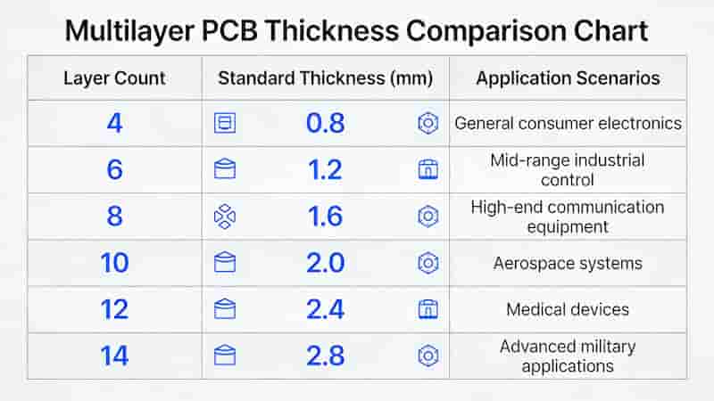
Industry standard thicknesses balance performance, cost and compatibility. Below is the official reference table for multilayer PCB stackup and thickness:
| Layer Count | Standard Thickness | Typical Range | Main Applications |
|---|---|---|---|
| 4‑Layer PCB | 1.6 mm (0.063″) | 1.0 – 2.4 mm | Industrial controls, consumer electronics, IoT |
| 6‑Layer PCB | 1.6 mm | 1.6 – 2.4 mm | High‑speed digital, MCU systems, interface boards |
| 8‑Layer PCB | 2.0 mm (0.079″) | 1.6 – 3.0 mm | Telecom, FPGA, dense computing |
| 10‑Layer PCB | 2.0 – 2.4 mm | 1.8 – 3.0 mm | Networking, backplanes, advanced embedded |
| 12‑Layer PCB | 2.0 – 2.4 mm | 2.0 – 3.0 mm | High‑density systems, multi‑interface devices |
| 14‑Layer PCB | 2.4 – 3.0 mm | 2.0 – 3.2 mm | Ultra high‑speed, complex SoC, multi‑plane designs |
4‑Layer to 14‑Layer Stackup And Thickness Details
4‑Layer PCB Stackup And Thickness
The most widely used multilayer PCB stackup for balanced performance and cost. Standard thickness: 1.6 mm.
- Typical stack: Top Signal → GND Plane → PWR Plane → Bottom Signal
- Standard thicknesses: 0.8 mm, 1.0 mm, 1.2 mm, 1.6 mm, 2.0 mm
- Best for: Industrial controls, IoT, consumer electronics, automotive modules
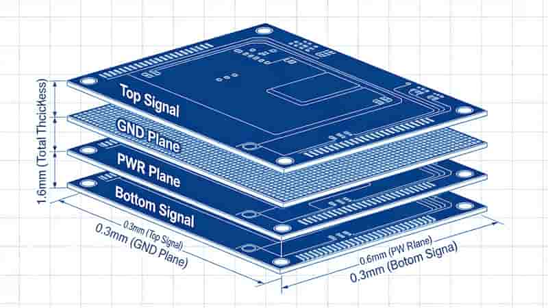
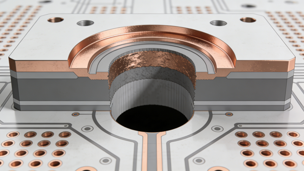
Standard 4‑Layer PCB Stackup Structure
6‑Layer PCB Stackup And Thickness
Enhanced EMC and impedance control for mid‑range high‑speed designs. Standard thickness: 1.6 mm.
Common stack uses dual ground planes to isolate signals and improve heat dissipation.
8‑Layer to 14‑Layer PCB Stackup And Thickness
High‑layer multilayer PCB stackup supports complex high‑speed signals, multiple power domains and strict EMI requirements. Thickness typically starts at 2.0 mm.
Symmetrical layer arrangement, dedicated reference planes and controlled dielectric thickness ensure stable impedance and reliable mass production.
Multilayer PCB Stackup Design Best Practices
- Use symmetrical stackup to prevent warpage and ensure consistent impedance
- Place ground planes adjacent to signal layers for optimal EMC and SI
- Select standard thickness to reduce cost and shorten lead time
- Match copper weight to current load and thermal requirements
- Confirm core/prepreg combinations with manufacturing capabilities early
- Use high‑Tg materials for high‑temperature and high‑reliability applications
PCB Stackup Design Best Practices
Conclusion
Multilayer PCB stackup and thickness are foundational to performance, reliability and manufacturability. Standard 4‑layer to 14‑layer configurations provide proven solutions for most industrial and high‑speed applications.
Choosing the right stackup requires balancing layer count, impedance, thickness, materials and manufacturing constraints. Following industry standards ensures lower cost, faster delivery and higher production yield.
Need Custom Multilayer PCB Stackup Support?
Our engineering team provides free stackup review, impedance optimization and thickness recommendation for your 4‑layer to 14‑layer PCB designs.
Get a free DFM check and custom quotation for your prototype or mass production project.
Request Free Stackup Design & Quote
Accelerate Your Innovation with Rapid PCB Prototyping
Fast Prototype PCB Manufacturing Services in Canada
Understanding Plated Half-Holes (Castellated Holes) in PCB Design
What is a Surface Mount Device or SMD Component Package?
What is FR-4 Material in PCB Fabrication? The Complete Professional Guide