PCB vias connect layers in multilayer circuit boards, enabling compact, high-performance electronics. This guide covers plated through holes, blind, and buried vias, their design, manufacturing, and advantages in modern PCB fabrication. From 5G devices to automotive systems, understand how to choose the right via type for your project.
What Are PCB Vias?
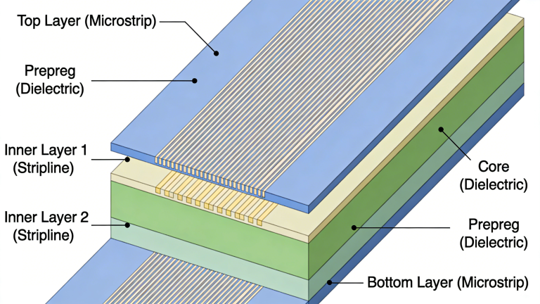
A PCB via is a small conductive hole in a multilayer PCB that connects copper circuits across different layers, allowing electrical signals to flow reliably. In modern electronics, multilayer PCBs deliver compactness and high performance for smartphones, medical devices, and automotive systems.
Copper layers are separated by insulation, so vias are essential to create stable interlayer connections. Without vias, complex circuits cannot function efficiently.
Vias support signal routing, power delivery, and component mounting. They are foundational to high-speed 5G, IoT, and industrial PCB designs.
Schematic diagram of various via holes in PCB
PCB Via Types
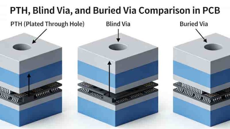
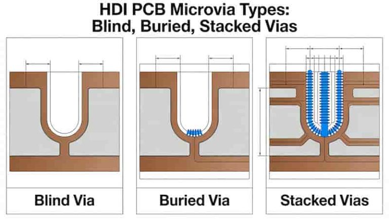
PCB vias enable layer connectivity in multilayer boards. Three main types—plated through holes, blind vias, and buried vias—match different design goals for density, performance, and cost.
Understanding each type helps engineers select the best solution for HDI, high-speed, and standard PCB designs.
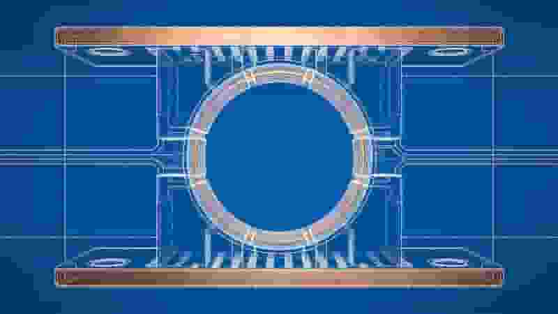
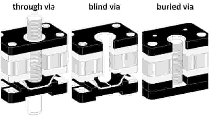
Various holes connect circuits in different layers
Plated Through Hole (PTH)
A Plated Through Hole (PTH) is a via that goes through the entire PCB thickness, connecting top to bottom layers with a copper-plated wall.
Made by mechanical drilling and plating, PTHs are the most affordable and widely used via type, with a minimum diameter of 0.15 mm.
They suit standard PCBs for consumer electronics, power supplies, and industrial controls.
Plated Through Hole (PTH)
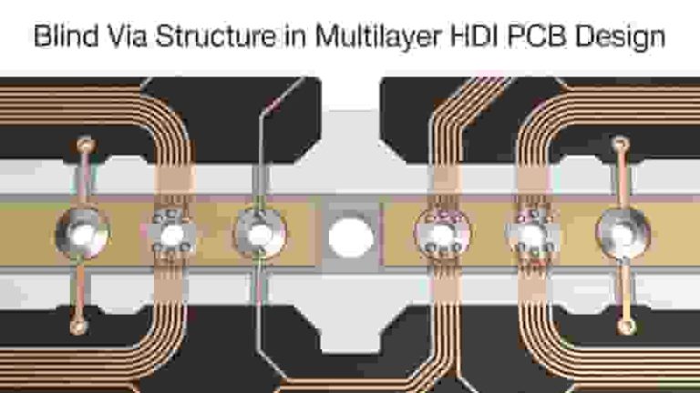
Blind Via Hole (BVH)
A Blind Via connects an outer PCB layer to inner layers without going through the entire board.
Created by laser drilling, blind vias support diameters down to 0.1 mm and improve routing space for HDI designs.
Ideal for mobile devices, wearables, and high-speed communication PCBs.
Blind Via Hole (BVH)
Buried Via Hole
A Buried Via connects only inner PCB layers and is fully enclosed inside the board.
Fabricated before lamination, these vias maximize surface space and signal integrity for high-layer-count designs.
Used in servers, aerospace, medical, and advanced HDI PCBs.
Buried Via Hole
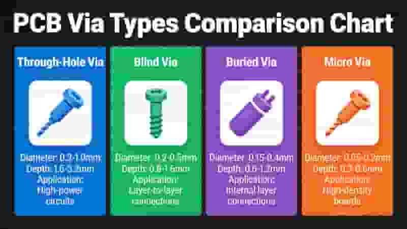
Comparison & Considerations
Each via type balances cost, density, and performance. The table below helps you choose the right type for your PCB project.
| Parameter | Through Via (PTH) | Blind Via | Buried Via |
|---|---|---|---|
| Connectivity | All layers | Outer to inner | Inner only |
| Visibility | Both sides | One side | Invisible |
| Min Size | 0.15 mm | 0.10 mm | 0.10 mm |
| Cost | Lowest | Medium | Highest |
| Best For | Standard PCBs | HDI & Mobile | High-Speed HDI |
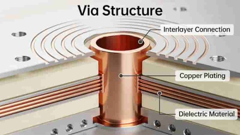
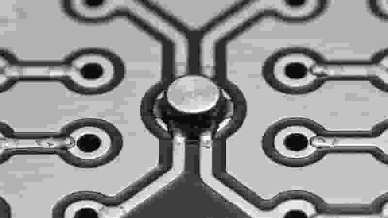
PCB Via Design & Manufacturing
PCB via performance depends on precise design and manufacturing. Drilling methods include mechanical for PTH and laser for blind/buried vias.
Depth-to-diameter ratios and copper plating ensure reliable conductivity. Following IPC standards guarantees consistent quality for industrial and high-speed PCBs.
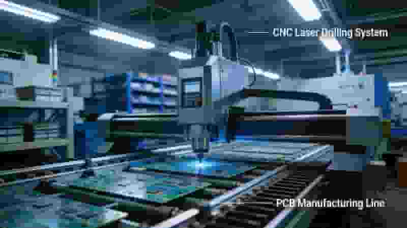
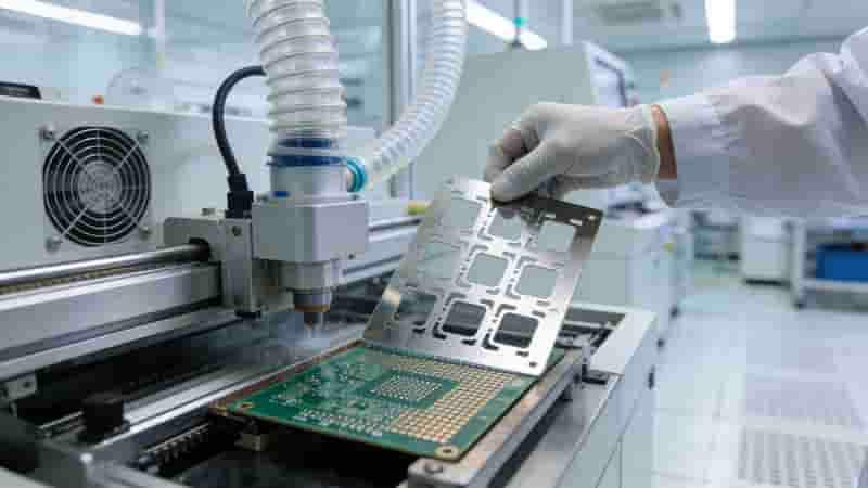
PCB CNC Drilling vs Laser Drilling
Advantages of Blind & Buried Vias
Blind and buried vias greatly improve PCB density and signal integrity. They save surface space, reduce interference, and support smaller form factors.
These vias are essential for 5G, automotive, and high-performance electronics where miniaturization and reliability matter most.
Conclusion
PCB vias are critical building blocks of modern multilayer PCBs. Choosing between through, blind, and buried vias directly impacts cost, size, and electrical performance.
With the right via design, you can optimize your PCB for 5G, automotive, industrial, and high-speed applications.
Need Professional PCB Manufacturing?
We provide high-quality PCB fabrication with expert via design, reliable HDI production, and global delivery.
Contact us today for a free quote and custom solution!

How to Find Reliable China PCB Manufacturers: 5 Critical Vetting Tips
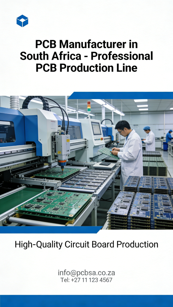
PCB Manufacturer in South Africa | Reliable Custom PCB & PCBA Services
The 10 Main Steps of the PCB Assembly Process | Full Professional Guide
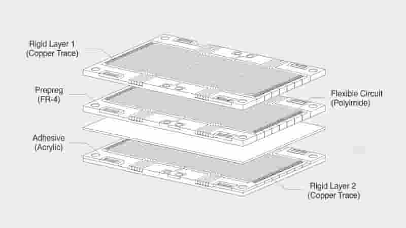
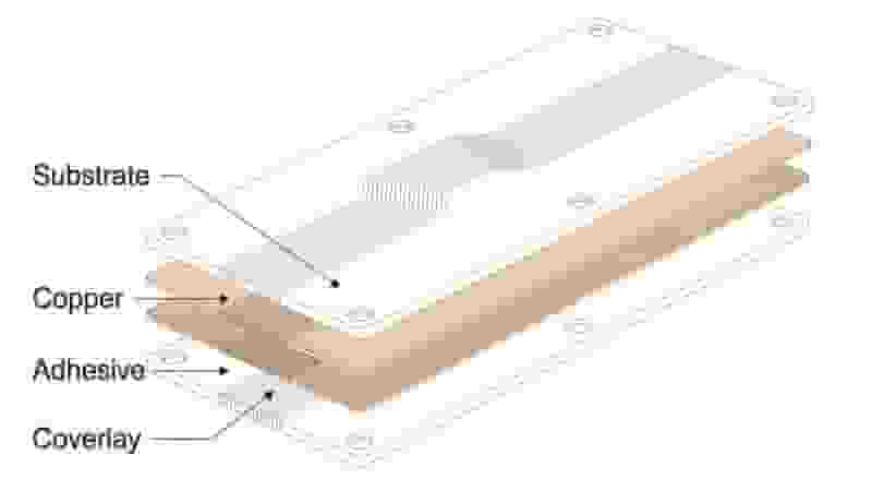
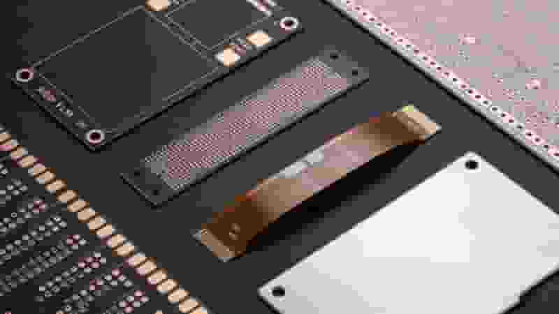
Rigid-Flex PCB Stackup: Professional Design & Manufacturing Guide
Fast Turnaround PCB Prototype Services from Certified Manufacturer