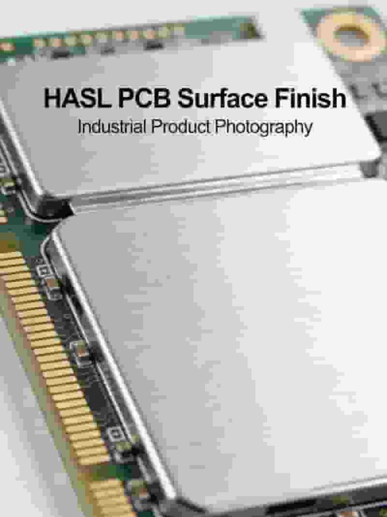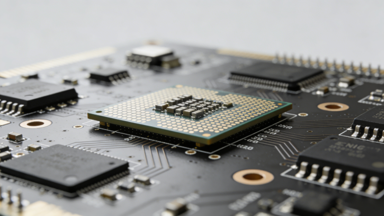
HASL (Hot Air Solder Leveling) is a widely used, cost-effective PCB surface finish that protects copper pads from oxidation and ensures reliable solderability for industrial and commercial electronics assembly.
What Is Hot Air Solder Leveling (HASL)?
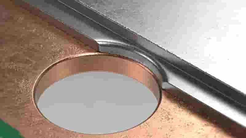
Hot Air Solder Leveling (HASL) is a mature and industry-standard PCB surface finish applied to exposed copper circuits. It coats pads with molten solder and uses high-pressure hot air to create a uniform protective layer, preventing oxidation and ensuring strong solder joints during assembly.
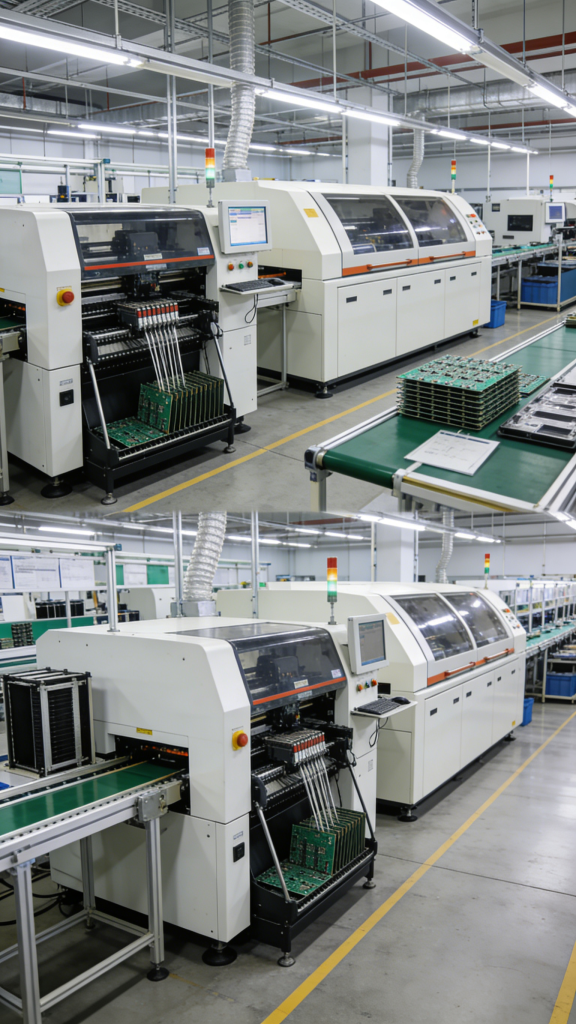
For decades, HASL has been the most widely adopted surface treatment due to its low cost, strong reliability, and compatibility with standard assembly processes. It supports both through-hole and SMT assembly, making it ideal for mass production and prototyping alike.
How the HASL Process Works
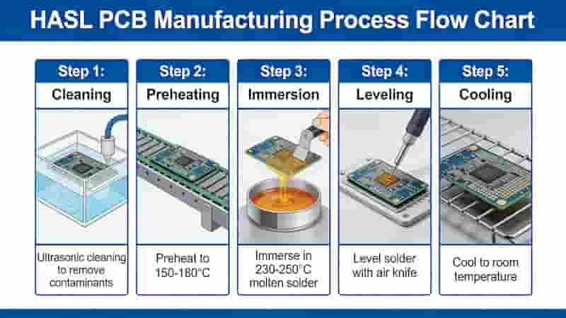
The HASL process follows a strict, repeatable workflow to ensure consistent coating quality across all PCB panels:
- Precleaning: Removes contaminants, oils, and oxides from copper surfaces.
- Preheating: Reduces thermal shock before solder immersion.
- Solder Immersion: PCB is dipped into molten solder alloy to coat copper pads.
- Hot Air Leveling: High-temperature air knives remove excess solder for uniformity.
- Cooling & Inspection: Rapid cooling stabilizes the finish; quality checks ensure performance.
Key Benefits of HASL for PCB Production
- Low Cost: Most economical PCB surface finish for high-volume runs.
- Excellent Solderability: Native solder layer ensures strong, stable joints.
- Long Shelf Life: Up to 12 months of sealed storage without degradation.
- Easy Rework: Supports multiple reflow cycles and field repairs.
- Universal Compatibility: Works with wave soldering, hand soldering, and standard SMT lines.
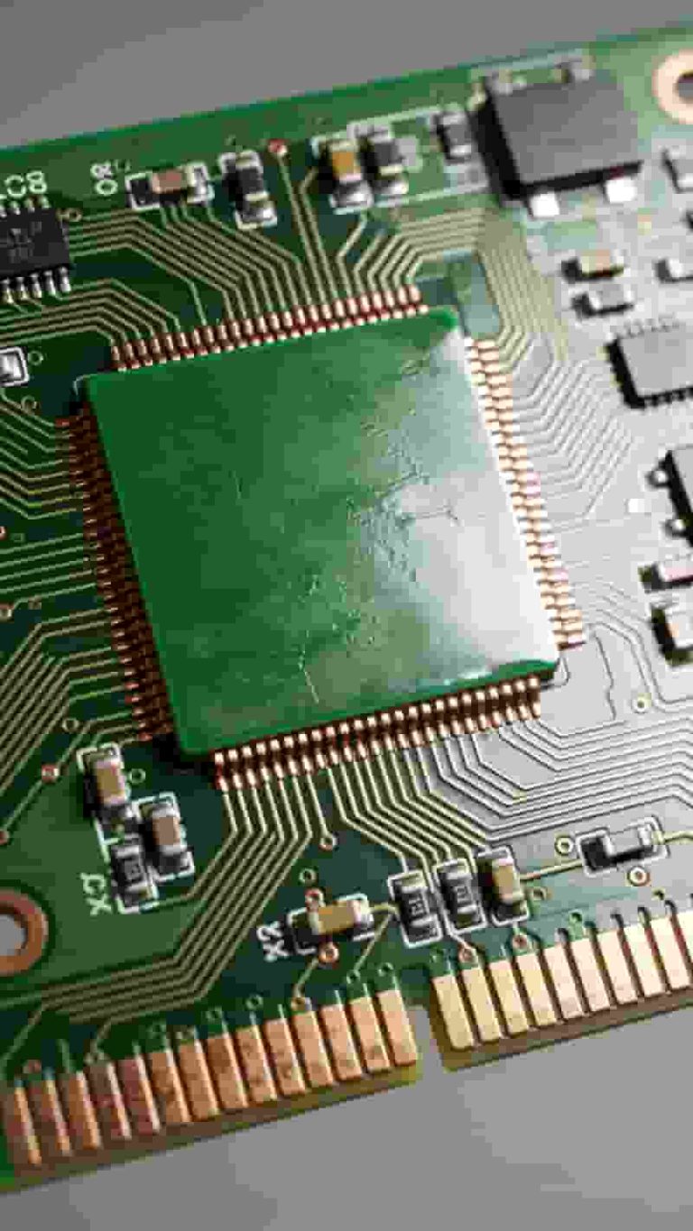
Limitations of HASL
- Moderate surface flatness; not recommended for fine-pitch components below 0.5mm.
- Higher processing temperature may stress thin or high-layer-count PCB substrates.
- Slight pad unevenness can affect precision stencil printing.
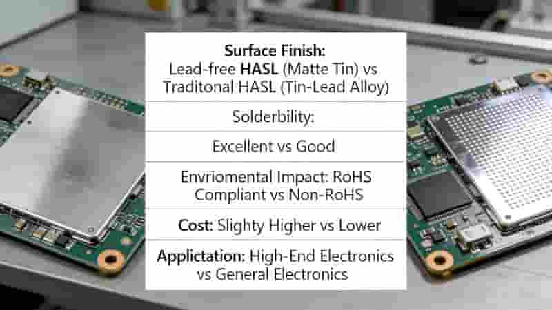
- Traditional leaded HASL is not RoHS-compliant for global markets.
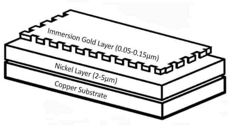
Lead-Free HASL vs Traditional HASL
Modern electronics require compliance with RoHS and REACH, making lead-free HASL the standard for global export. Below are the core differences:
| Item | Traditional HASL | Lead-Free HASL |
|---|---|---|
| Alloy | 63% Sn + 37% Pb | SnCu or SAC305 |
| RoHS | No | Yes |
| Melting Point | Low | High |
| Best For | Legacy, non-regulated markets | Global export, industrial electronics |
HASL vs Other PCB Surface Finishes
| Finish | Cost | Flatness | Fine Pitch | RoHS |
|---|---|---|---|---|
| HASL | Low | Moderate | ≥0.5mm | LF Version |
| ENIG | High | Excellent | <0.5mm | Yes |
| OSP | Low | Excellent | Good | Yes |

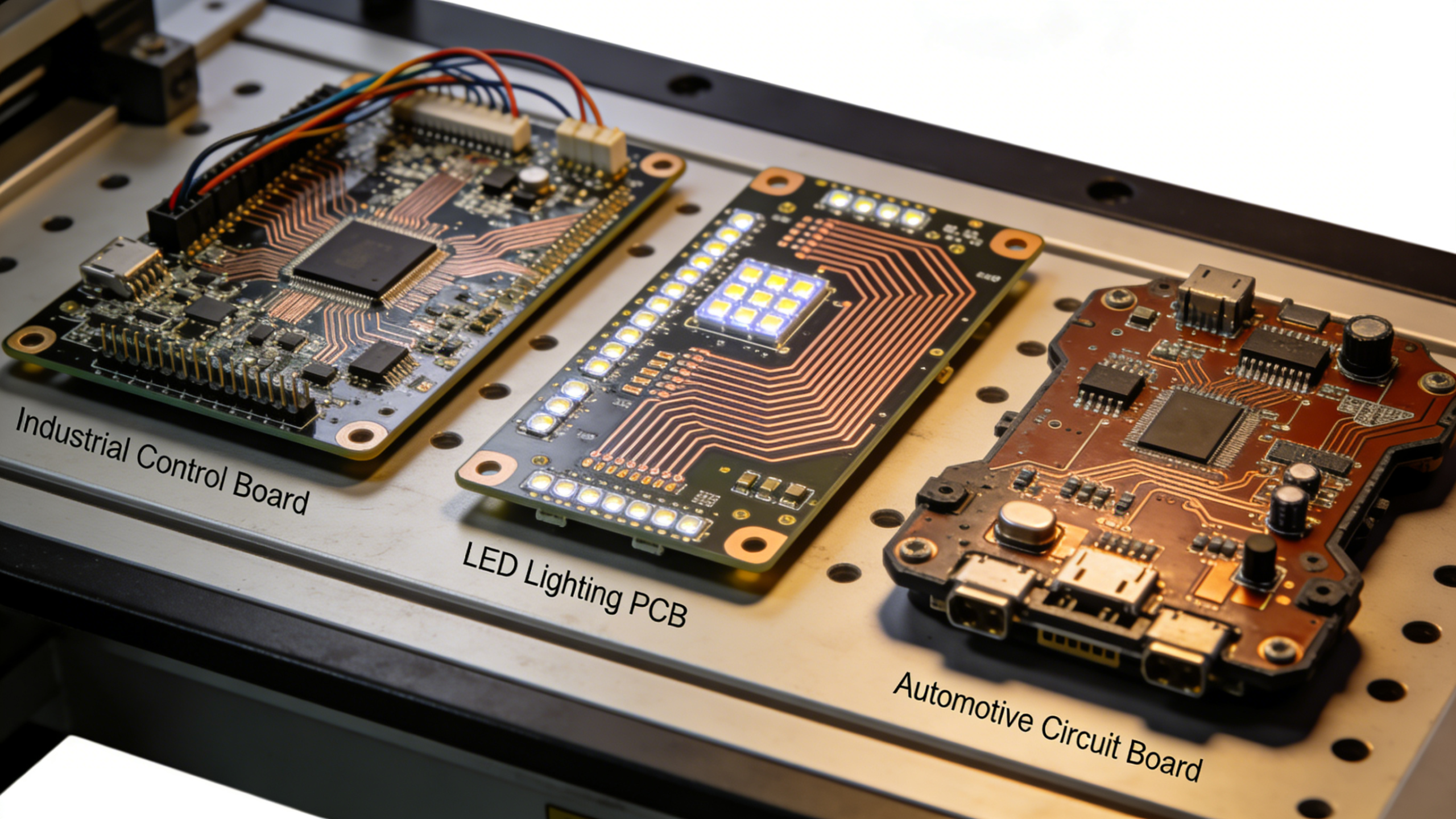
Ideal Applications for HASL PCBs
HASL is widely used in industrial and commercial electronics where cost and reliability are critical:
- Industrial control and power supply PCB
- LED lighting and consumer electronics
- Automotive non-safety subsystems
- Through-hole heavy assemblies
- Prototypes and mid-volume production
- General-purpose boards for global markets

Conclusion
HASL remains one of the most practical and cost-efficient PCB surface finish options available today. With lead-free HASL, it meets global environmental standards while delivering consistent solderability and protection for copper circuits.
It is the top choice for cost-sensitive projects, industrial equipment, and standard SMT/through-hole assemblies where ultra-fine pitch is not required.
Get Your HASL PCB Quote Today
We provide professional HASL and lead-free HASL PCB manufacturing for global buyers. Send your Gerber files and BOM for a fast, free, and detailed quotation.
Inquire Now | Free PCB Quote
Double-sided PCB Manufacturing Process – We Deliver Compliant, Efficient Production
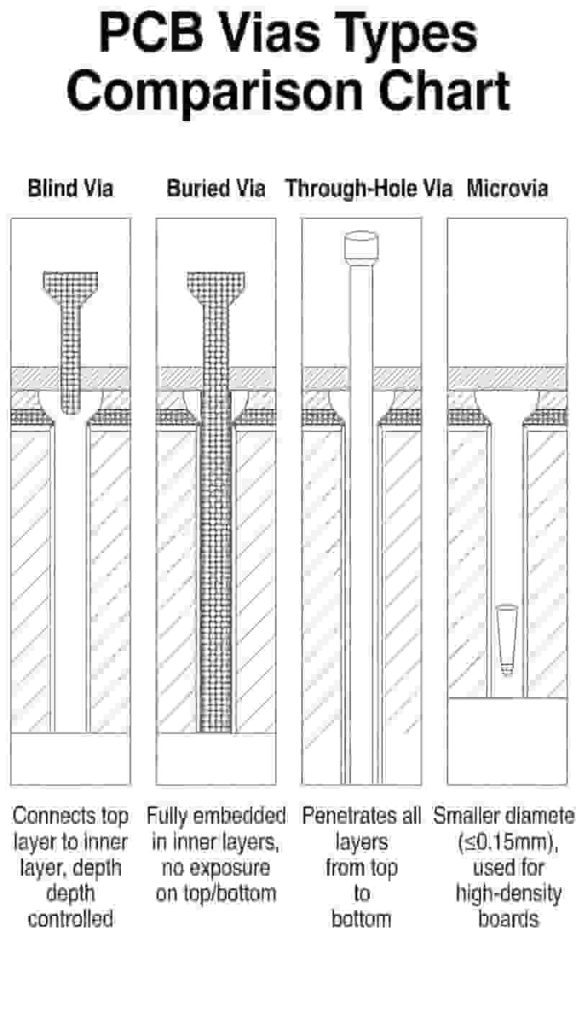
PCB Vias: Complete Overview, Types, Design & Manufacturing for Engineers & Buyers
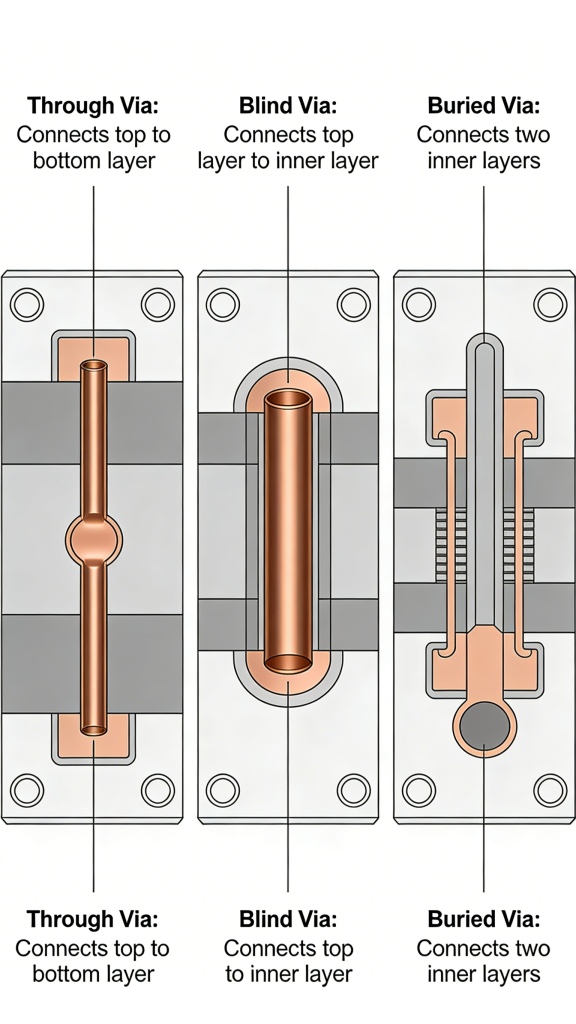
PCB Vias Explained: Through, Blind, and Buried HolesPCB
Turnkey PCB Assembly Services | Full & Partial Solutions
What Are Tented Vias? A Complete PCB Design Guide